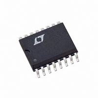
LTC1596-1CCSW Linear Technology, LTC1596-1CCSW Datasheet - Page 10

LTC1596-1CCSW
Manufacturer Part Number
LTC1596-1CCSW
Description
IC D/A CONV 16BIT MLTPLYNG16SOIC
Manufacturer
Linear Technology
Datasheet
1.LTC1595CCS8PBF.pdf
(12 pages)
Specifications of LTC1596-1CCSW
Settling Time
1µs
Number Of Bits
16
Data Interface
Serial
Number Of Converters
1
Voltage Supply Source
Single Supply
Power Dissipation (max)
55µW
Operating Temperature
0°C ~ 70°C
Mounting Type
Surface Mount
Package / Case
16-SOIC (0.300", 7.5mm Width)
Lead Free Status / RoHS Status
Contains lead / RoHS non-compliant
APPLICATIONS
LTC1595/LTC1596/LTC1596-1
Bipolar (4-Quadrant Multiplying) Mode
(V
The LTC1595/LTC1596 can be used with a dual op amp
and three external resistors to provide 4-quadrant multi-
plying operation as shown in Figure 2 (last page). With a
fixed 10V reference, the circuits shown give a precision
bipolar –10V to 10V output swing. Using the LTC1596-1
will cause the power-on reset and clear pin to reset the DAC
to midscale (bipolar zero).
Op Amp Selection
Because of the extremely high accuracy of the 16-bit
LTC1595/LTC1596, thought should be given to op amp
selection in order to achieve the exceptional performance
of which the part is capable. Fortunately, the sensitivity of
INL and DNL to op amp offset has been greatly reduced
compared to previous generations of multiplying DACs.
Op amp offset will contribute mostly to output offset and
gain and will have minimal effect on INL and DNL. For
example, a 500 V op amp offset will cause about 0.55LSB
10
Table 2. 16-Bit Settling Time for Various Amplifiers Driven by the LT1595 DAC. LT1468 (Shaded) Offers Fastest Settling Time While
Maintaining Accuracy Over Temperature
AMPLIFIER
LT1001
LT1007
LT1013
LT1077
LT1097
LT1112
LT1178
LT1468
OUT
= – V
REF
to V
U
REF
)
CONSERVATIVE SETTLING TIME
INFORMATION
AND COMPENSATION VALUE
U
120 s
200 s
120 s
120 s
450 s
2.5 s
19 s
75 s
W
100pF
100pF
150pF
100pF
100pF
100pF
75pF
30pF
U
COMMENTS
Good Low Speed Choice
I
Good Low Speed Choice
Good Low Speed Choice Dual
Low Power Dual
Fastest Settling with 16-Bit Performance
INL degradation and 0.15LSB DNL degradation with a 10V
full-scale range. The main effects of op amp offset will be
a degradation of zero-scale error equal to the op amp
offset, and a degradation of full-scale error equal to twice
the op amp offset. For example, the same 500 V op amp
offset will cause a 3.3LSB zero-scale error and a 6.5LSB
full-scale error with a 10V full-scale range.
Op amp input bias current (I
scale error equal to I
Table 2 shows a selection of LTC op amps which are
suitable for use with the LTC1595/LTC1596. For a thor-
ough discussion of 16-bit DAC settling time and op amp
selection, refer to Application Note 74, “ Component and
Measurement Advances Ensure 16-Bit DAC Settling Time. ”
Grounding
As with any high resolution converter, clean grounding is
important. A low impedance analog ground plane and star
grounding should be used. I
(LTC1595) must be tied to the star ground with as low a
resistance as possible.
B
1LSB Error Due to V
Gives 1LSB Error at 25 C
OS
over Temperature
BIAS
(R
FB
BIAS
) = I
OUT2
) contributes only a zero-
BIAS
(LTC1596) and GND
(R
REF
) = I
BIAS
(7k).


