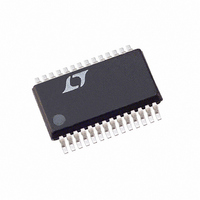
LTC1668CG Linear Technology, LTC1668CG Datasheet - Page 12

LTC1668CG
Manufacturer Part Number
LTC1668CG
Description
IC D/A CONV 16BIT 50MSPS 28-SSOP
Manufacturer
Linear Technology
Datasheet
1.LTC1668CGPBF.pdf
(24 pages)
Specifications of LTC1668CG
Settling Time
20ns
Number Of Bits
16
Data Interface
Parallel
Number Of Converters
1
Voltage Supply Source
Dual ±
Power Dissipation (max)
180mW
Operating Temperature
0°C ~ 70°C
Mounting Type
Surface Mount
Package / Case
28-SSOP
Lead Free Status / RoHS Status
Contains lead / RoHS non-compliant
Other names
Q1158656A
Available stocks
Company
Part Number
Manufacturer
Quantity
Price
Part Number:
LTC1668CG
Manufacturer:
LINEAR/凌特
Quantity:
20 000
Company:
Part Number:
LTC1668CG#PBF
Manufacturer:
LTC
Quantity:
733
Part Number:
LTC1668CG#PBF
Manufacturer:
LINEAR/凌特
Quantity:
20 000
LTC1666/LTC1667/LTC1668
APPLICATIO S I FOR ATIO
Adjusting the Full-Scale Output
In Figure 2, a serial interfaced DAC is used to set I
The LTC1661 is a dual 10-bit V
voltage output that swings from 0V to V
DAC Transfer Function
The LTC1666/LTC1667/LTC1668 use straight binary digital
coding. The complementary current outputs, I
B
nal), I
Code = 0) to 10mA when all bits are high (e.g., Code = 65535
for LTC1668) (decimal representation). I
mentary to I
formulas:
LTC1666:
LTC1667:
LTC1668:
In typical applications, the LTC1666/LTC1667/LTC1668
differential output currents either drive a resistive load
directly or drive an equivalent resistive load through a
transformer, or as the feedback resistor of an I-to-V
converter. The voltage outputs generated by the I
I
12
OUT B
, sink current from 0 to I
I
I
I
I
I
I
OUT A
OUT B
OUT A
OUT B
OUT A
OUT B
OUT A
output currents are then:
Figure 2. Adjusting the Full-Scale Current of
the LTC1666/LTC1667/LTC1668 with a DAC
= I
= I
= I
= I
= I
= I
5V
OUT A
swings from 0mA when all bits are low (e.g.,
OUTFS
OUTFS
OUTFS
OUTFS
OUTFS
OUTFS
1/2 LTC1661
. I
OUT A
• (DAC Code/4096)
• (4095 – DAC Code)/4096
• (DAC Code/16384)
• (16383 – DAC Code)/16384
• (DAC Code/65536)
• (65535 – DAC Code)/65536
REF
U
and I
OUTFS
U
0.1 F
OUT B
R
. For I
1.9k
SET
OUT
are given by the following
W
OUTFS
DAC with a buffered
I
REFIN
REFERENCE
REF
OUT B
+
–
2.5V
= 10mA (nomi-
.
OUT A
LTC1666/
LTC1667/
LTC1668
is comple-
U
1666/7/8
OUT A
and I
OUTFS
F03
and
OUT
(2)
(3)
(4)
(5)
(6)
(7)
.
The differential voltage is:
Substituting the values found earlier for I
I
From these equations some of the advantages of differen-
tial mode operation can be seen. First, any common mode
noise or error on I
signal power is twice as large as in the single-ended case.
Third, any errors and noise that multiply times I
I
midscale, where AC signal waveforms tend to spend the
most time. Fourth, this transfer function is bipolar; e.g. the
output swings positive and negative around a zero output
at mid-scale input, which is more convenient for AC
applications.
Note that the term (R
differential and single-ended transfer functions. This means
that the Gain Error of the DAC depends on the ratio of
R
temperature tracking of R
the absolute tempco of R
nonlinearity. As the DAC output changes from 0mA to
10mA the R
very low tempco can produce enough INL bowing to be
significant at the 16-bit level. This effect disappears with
medium to high frequency AC signals due to the slow
thermal time constant of the load resistor.
Analog Outputs
The LTC1666/LTC1667/LTC1668 have two complemen-
tary current outputs, I
Function). The output impedance of I
(R
Figure 3.)
OUTFS
OUT B
LOAD
IOUT A
V
V
V
V
(R
OUT A
OUT B
DIFF
DIFF
LOAD
, such as reference or I
to R
(LTC1668):
= V
= (I
= {2 • DAC Code – 65535)/65536} • 8 •
and R
/R
= I
= I
SET
OUT A
OUT A
LOAD
SET
OUT A
OUT B
, and the Gain Error tempco is affected by the
IOUT B
) • (V
resistor will heat up slightly, and even a
OUT A
– V
– I
• R
• R
) is typically 1.1k to LADCOM. (See
OUT B
REF
OUT B
LOAD
LOAD
OUT A
and I
LOAD
)
) • (R
LOAD
OUT B
LOAD
and I
/R
SET
LOAD
OUTFS
with R
is cancelled. Second, the
OUT B
is very critical for DC
) appears in both the
)
noise, cancel near
SET
(see DAC Transfer
OUT A
OUT A
. Note also that
, I
and I
OUT A
OUT B
OUT B
(10)
(11)
and
and
(8)
(9)


