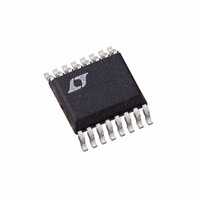
LTC2604IGN#PBF Linear Technology, LTC2604IGN#PBF Datasheet - Page 5

LTC2604IGN#PBF
Manufacturer Part Number
LTC2604IGN#PBF
Description
IC DAC 16BIT QUAD R-R OUT 16SSOP
Manufacturer
Linear Technology
Datasheet
1.LTC2624IGN-1PBF.pdf
(16 pages)
Specifications of LTC2604IGN#PBF
Settling Time
10µs
Number Of Bits
16
Data Interface
Serial
Number Of Converters
4
Voltage Supply Source
Single Supply
Power Dissipation (max)
10mW
Operating Temperature
-40°C ~ 85°C
Mounting Type
Surface Mount
Package / Case
16-SSOP
Lead Free Status / RoHS Status
Lead free / RoHS Compliant
Available stocks
Company
Part Number
Manufacturer
Quantity
Price
SYMBOL
t
TYPICAL PERFORMANCE CHARACTERISTICS
(LTC2604/LTC2604-1, LTC2614/LTC2614-1, LTC2624/LTC2624-1)
TIMING CHARACTERISTICS
range, otherwise specifi cations are at T
= 2.048V (V
Note 1: Stresses beyond those listed under Absolute Maximum Ratings
may cause permanent damage to the device. Exposure to any Absolute
Maximum Rating condition for extended periods may affect device
reliability and lifetime.
Note 2: Linearity and monotonicity are defi ned from code k
2
rounded to the nearest whole code. For V
k
Note 3: Digital inputs at 0V or V
Note 4: DC crosstalk is measured with V
the measured DAC at midscale, unless otherwise noted.
10
N
L
–0.02
–0.04
–0.06
–0.08
–0.10
= 256, linearity is defi ned from code 256 to code 65,535.
– 1, where N is the resolution and k
0.10
0.08
0.06
0.04
0.02
2.5
2.0
1.5
1.0
0.5
0
3
0
–40 –30 –20 –10
–50
Current Limiting
Zero-Scale Error vs Temperature
CODE = MIDSCALE
–30
CC
PARAMETER
CS/LD High to SCK Positive Edge
SCK Frequency
= 2.5V), REF LO = 0V, V
–10
TEMPERATURE (°C)
V
V
V
V
REF
REF
REF
REF
I
= V
= V
10
OUT
= V
= V
CC
CC
CC
CC
0
(mA)
= 5V
= 3V
30
= 3V
= 5V
CC
10
.
50
20
L
is given by k
CC
REF
70
30
2604 G01
2604 G04
= 5V and V
OUT
= 4.096V and N = 16,
A
40
90
= 25°C. REF A = REF B = REF C = REF D = 4.096V (V
unloaded, unless otherwise noted. (Note 10)
L
REF
= 0.016(2
–0.2
–0.4
–0.6
–0.8
–1.0
–0.1
–0.2
–0.3
–0.4
1.0
0.8
0.6
0.4
0.2
0.4
0.3
0.2
0.1
= 4.096V, with
0
L
0
–35
–50
to code
Load Regulation
Gain Error vs Temperature
CODE = MIDSCALE
V
The
REF
N
CONDITIONS
50% Duty Cycle
/V
–25
–30
= V
REF
●
CC
denotes specifi cations which apply over the full operating temperature
),
–15
–10
= 5V
TEMPERATURE (°C)
V
REF
I
–5
10
OUT
= V
Note 5: R
Note 6: Guaranteed by design and not production tested.
Note 7: Inferred from measurement at code 256 (LTC2604), code 64
(LTC2614) or code 16 (LTC2624), and at full scale.
Note 8: V
3/4 scale to 1/4 scale. Load is 2k in parallel with 200pF to GND.
Note 9: V
and half scale –1. Load is 2k in parallel with 200pF to GND.
Note 10: These specifi cations apply to LTC2604/LTC2604-1, LTC2614/
LTC2614-1, LTC2624/LTC2624-1.
(mA)
CC
30
5
LTC2604/LTC2614/LTC2624
= 3V
15
50
L
CC
CC
= 2kΩ to GND or V
= 5V, V
= 5V, V
25
70
2604 G02
2604 G05
REF
REF
35
90
= 4.096V. DAC is stepped 1/4 scale to 3/4 scale and
= 4.096V. DAC is stepped 1LSB between half scale
CC
l
l
= 5V), REF A = REF B = REF C = REF D
CC
–1
–2
–3
–1
–2
–3
3
2
1
0
3
2
1
0
–50
2.5
.
Offset Error vs Temperature
Offset Error vs V
MIN
–30
7
3
–10
TEMPERATURE (°C)
3.5
TYP
10
V
CC
CC
4
(V)
30
MAX
4.5
50
50
5
70
2604 G03
2604 G06
UNITS
2604fd
5
MHz
5.5
90
ns


