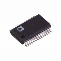
AD7805BRSZ Analog Devices Inc, AD7805BRSZ Datasheet - Page 17

AD7805BRSZ
Manufacturer Part Number
AD7805BRSZ
Description
IC DAC 10BIT QUAD PARALL 28-SSOP
Manufacturer
Analog Devices Inc
Datasheet
1.AD7808BRZ.pdf
(28 pages)
Specifications of AD7805BRSZ
Data Interface
Parallel
Settling Time
1.5µs
Number Of Bits
10
Number Of Converters
4
Voltage Supply Source
Analog and Digital
Power Dissipation (max)
66mW
Operating Temperature
-40°C ~ 85°C
Mounting Type
Surface Mount
Package / Case
28-SSOP
Resolution (bits)
10bit
Sampling Rate
667kSPS
Input Channel Type
Parallel
Supply Voltage Range - Analogue
3V To 5.5V
Supply Voltage Range - Digital
3V To 5.5V
Supply
RoHS Compliant
Lead Free Status / RoHS Status
Lead free / RoHS Compliant
Available stocks
Company
Part Number
Manufacturer
Quantity
Price
Part Number:
AD7805BRSZ
Manufacturer:
ADI/亚德诺
Quantity:
20 000
REV. A
Table VII shows the twos complement transfer function for the
Sub DAC. Figure 23 shows the Sub DAC transfer function for
twos complement coding. Any Sub DAC output voltage can be
expressed as:
where NB is the decimal equivalent of the twos complement
input code. NB ranges from –128 to +127.
Figure 23. Sub DAC Output Voltage vs. DAC Input Codes
(HEX) for Twos Complement Coding
The total output for a single channel when using twos comple-
ment coding is the sum of the voltage from the Main DAC and
the Sub DAC.
V
where NA ranges from –512 to +511 and NB ranges from –128 to
+127. Figure 28 shows a pictorial view of the transfer function for
any DAC.
OUT
Table VII. Twos Complement Code Table for Sub DAC
DAC INPUT CODE
= V
= V
= V
BIAS
127
128
OUT
BIAS
256
256
Digital Input
MSB . . . LSB
01111111
01111111
00000001
00000000
11111111
10000001
10000000
' + V
+ 1.875 V
V
V
BIAS
BIAS
16
16
(1 + 1.875 NA/1024 + NB/4096)
0
V
OUT
80
OUT
"
" = V
81
BIAS
BIAS
Analog Input
(V
(V
(V
0
(–V
(–V
(–V
(NA/1024) + V
/16
BIAS
BIAS
BIAS
BIAS
BIAS
BIAS
FF 00
/16)
/16)
/16)
(NB/256)
/16)
/16)
/16)
01
(127/256)
(126/256)
(1/256)
(1/256)
(127/256)
(128/256)
BIAS
/16 (NB/256)
7E
7F
–17–
Configuring the AD7805/AD7809 for Twos Complement Coding
Figure 24 shows a typical configuration for the AD7805/AD7809.
The circuit can be used for either 3.3 V or 5 V operation and uses
the internal V
lel interfacing is used. The following are the steps required to
operate the Main DACs in this part.
System Control Register Write:
Channel Control Register Write:
DAC Data Register Write:
MODE = 0, address inputs (A2, A1, A0) are don’t cares.
MODE = 0, address inputs (A2, A1, A0) select desired channel.
MODE = 1, address inputs (A2, A1, A0) select desired channel.
Figure 24. Typical Configuration for AD7805/AD7809
Write 020 Hex
Write 011 Hex
Write XXX Hex With MODE = 1 all data writes are to
AD7804/AD7805/AD7808/AD7809
INTERFACE
DIGITAL
DD
0.01 F
0.01 F
DV
/2 as the reference for the part and 10-bit paral-
DD
*USED ON THE
AD7809 ONLY
10 F
complement coding, normal operation
DAC, and any DAC data writes that
follow are to the Main DAC.
the selected DAC. XXX is the required
data. 200 Hex will give zero scale and 1FF
Hex will give full scale from the DAC.
Configure part for 10-bit parallel, twos
Internal V
COMP
A0
A1
A2*
D9
D0
MODE
CS
WR
CLR
LDAC
0.1 F
DD
+3.3V/+5V
DGND
AV
AD7805/
AD7809
/2 selected as V
DD
DV
AGND
DD
REFOUT
V
V
V
V
REFIN
OUT
OUT
OUT
OUT
0.1 F
A
B
C
D
BIAS
for


