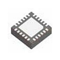
LM48511SQ National Semiconductor, LM48511SQ Datasheet - Page 9

LM48511SQ
Manufacturer Part Number
LM48511SQ
Description
Manufacturer
National Semiconductor
Datasheet
1.LM48511SQ.pdf
(22 pages)
Specifications of LM48511SQ
Operational Class
Class-D
Audio Amplifier Output Configuration
1-Channel Mono
Output Power (typ)
6.7x1@4OhmW
Audio Amplifier Function
Speaker
Single Supply Voltage (typ)
Not RequiredV
Dual Supply Voltage (typ)
5V
Power Supply Requirement
Triple
Rail/rail I/o Type
No
Power Supply Rejection Ratio
88dB
Single Supply Voltage (min)
Not RequiredV
Single Supply Voltage (max)
Not RequiredV
Dual Supply Voltage (min)
3/4.8V
Dual Supply Voltage (max)
5.5/8V
Operating Temp Range
-40C to 85C
Operating Temperature Classification
Industrial
Mounting
Surface Mount
Pin Count
24
Lead Free Status / Rohs Status
Not Compliant
Available stocks
Company
Part Number
Manufacturer
Quantity
Price
Part Number:
LM48511SQ
Manufacturer:
TI/德州仪器
Quantity:
20 000
Company:
Part Number:
LM48511SQ/NOPB
Manufacturer:
VTI
Quantity:
1 928
Company:
Part Number:
LM48511SQX/NOPB
Manufacturer:
NSC
Quantity:
1 720
PSRR
CMRR
η
V
FB
Note 1: “Absolute Maximum Ratings” indicate limits beyond which damage to the device may occur, including inoperability and degradation of device reliability
and/or performance. Functional operation of the device and/or non-degradation at the Absolute Maximum Ratings or other conditions beyond those indicated in
the Recommended Operating Conditions is not implied. TheRecommended Operating Conditions indicate conditions at which the device is functional and the
device should not be operated beyond such conditions. All voltages are measured with respect to the ground pin, unless otherwise specified.
Note 2: The Electrical Characteristics tables list guaranteed specifications under the listed Recommended Operating Conditions except as otherwise modified
or specified by the Electrical Characteristics Conditions and/or Notes. Typical specifications are estimations only and are not guaranteed.
Note 3: The maximum power dissipation must be derated at elevated temperatures and is dictated by T
allowable power dissipation is P
derating curves for additional information.
Note 4: Human body model, applicable std. JESD22-A114C.
Note 5: Machine model, applicable std. JESD22-A115-A.
Note 6: Typical values represent most likely parametric norms at T
characterization and are not guaranteed.
Note 7: Datasheet min/max specification limits are guaranteed by test or statistical analysis.
Note 8: Shutdown current is measured with components R1 and R2 removed.
Note 9: Feedback pin reference voltage is measured with the Audio Amplifier disconnected from the Boost converter (the Boost converter is unloaded).
Note 10: R
15μH+4Ω+15μH.
Note 11: Offset voltage is determined by: (I
Symbol
L
is a resistive load in series with two inductors to simulate an actual speaker load for R
Power Supply Rejection Ratio
(Input Referred)
Common Mode Rejection Ratio
(Input Referred)
Efficiency
Feedback Pin Reference Voltage
DMAX
= (T
Parameter
JMAX
DD (with load)
- T
A
) / θ
JA
— I
or the number given in Absolute Maximum Ratings, whichever is lower. For the LM48511, see power
DD (no load)
A
) x R
V
f
V
f
V
f
V
f = 1kHz, R
= +25ºC, and at the Recommended Operation Conditions at the time of product
RIPPLE =
RIPPLE =
RIPPLE =
RIPPLE
RIPPLE
RIPPLE
RIPPLE
FF
SS
FF
SS
FF
SS
L
.
= 200mV
= 200mV
= 200mV
= 1V
= 217Hz
= 1kHz
= 10kHz
9
L
Conditions
P-P
= 8Ω, P
, f
P-P
P-P
P-P
RIPPLE
Sine,
Sine,
Sine,
O
= 1W
= 217Hz
L
= 8Ω, the load is 15μH+8Ω+15μH. For R
JMAX
, θJ
JA
, and the ambient temperature, T
(Note 6)
Typical
1.23
89
89
88
88
78
78
71
75
LM48511
(Note 7)
Limit
L
= 4Ω, the load is
A
. The maximum
www.national.com
(Limits)
Units
dB
dB
dB
dB
dB
dB
dB
%
V


