AD5391BSTZ-5 Analog Devices Inc, AD5391BSTZ-5 Datasheet - Page 16
AD5391BSTZ-5
Manufacturer Part Number
AD5391BSTZ-5
Description
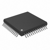
IC DAC 12BIT 16CHAN 3V 52LQFP
Manufacturer
Analog Devices Inc
Specifications of AD5391BSTZ-5
Data Interface
I²C, Serial
Design Resources
8 to 16 Channels of Programmable Voltage with Excellent Temperature Drift Performance Using AD5390/1/2 (CN0029) AD5390/91/92 Channel Monitor Function (CN0030)
Settling Time
6µs
Number Of Bits
12
Number Of Converters
16
Voltage Supply Source
Single Supply
Power Dissipation (max)
35mW
Operating Temperature
-40°C ~ 85°C
Mounting Type
Surface Mount
Package / Case
52-LQFP
Resolution (bits)
12bit
Sampling Rate
167kSPS
Input Channel Type
Serial
Supply Voltage Range - Analogue
4.5V To 5.5V
Supply Voltage Range - Digital
2.7V To 5.5V
Lead Free Status / RoHS Status
Lead free / RoHS Compliant
For Use With
EVAL-AD5391EBZ - BOARD EVALUATION FOR AD5391
Lead Free Status / RoHS Status
Lead free / RoHS Compliant, Lead free / RoHS Compliant
Available stocks
Company
Part Number
Manufacturer
Quantity
Price
Company:

Part Number:
AD5391BSTZ-5
Manufacturer:
Analog Devices Inc
Quantity:
10 000
Part Number:
AD5391BSTZ-5
Manufacturer:
ADI/亚德诺
Quantity:
20 000


AD5390/AD5391/AD5392
Mnemonic
PD
SPI/I
SCLK/SCL
DIN/SDA
Exposed Pad
(LFCSP only)
2
C
Function
Power-Down (level-sensitive, active high). Used to place the device in low power mode, in which the device consumes
1 μA analog current and 20 μA digital current. In power-down mode, all internal analog circuitry is placed in low power
mode; the analog output is configured as high impedance outputs or provides a 100 kΩ load to ground, depending on
how the power-down mode is configured. The serial interface remains active during power-down.
Interface Select Input Pin. When this input is low, I
Interface Clock Input Pin. In SPI-compatible serial interface mode, this pin acts as a serial clock input. It operates at clock
speeds up to 50 MHz.
I
compatible with both 100 kHz and 400 kHz operating modes.
Interface Data Input Pin.
SPI/I
SPI/I
This pad should be connected to the ground plane.
2
C mode: In I
2
2
C = 1: This pin acts as the serial data input. Data must be valid on the falling edge of SCLK.
C = 0, I
2
C mode: In I
2
C mode, this pin performs the SCL function, clocking data into the device. Data transfer rate in I
2
C mode, this pin is the serial data pin (SDA) operating as an open drain input/output.
Rev. C | Page 16 of 40
2
C mode is selected. When this input is high, SPI mode is selected.
2
C mode is
Related parts for AD5391BSTZ-5
Image
Part Number
Description
Manufacturer
Datasheet
Request
R

Part Number:
Description:
Wideband Dual-Channel Linear Multiplier/Divider
Manufacturer:
AD [Analog Devices]
Datasheet:

Part Number:
Description:
±1.7g Dual-Axis IMEMS Accelerometer Evaluation Board
Manufacturer:
Analog Devices Inc
Datasheet:

Part Number:
Description:
Inertial Sensor Evaluation System
Manufacturer:
Analog Devices Inc
Datasheet:
Part Number:
Description:
Manufacturer:
Analog Devices Inc
Datasheet:
Part Number:
Description:
Manufacturer:
Analog Devices Inc
Datasheet:
Part Number:
Description:
Manufacturer:
Analog Devices Inc
Datasheet:
Part Number:
Description:
Manufacturer:
Analog Devices Inc
Datasheet:
Part Number:
Description:
Manufacturer:
Analog Devices Inc
Datasheet:
Part Number:
Description:
Manufacturer:
Analog Devices Inc
Datasheet:
Part Number:
Description:
Manufacturer:
Analog Devices Inc
Datasheet:
Part Number:
Description:
Manufacturer:
Analog Devices Inc
Datasheet:
Part Number:
Description:
Manufacturer:
Analog Devices Inc
Datasheet:
Part Number:
Description:
Manufacturer:
Analog Devices Inc
Datasheet: