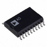
DAC8426FS Analog Devices Inc, DAC8426FS Datasheet

DAC8426FS
Specifications of DAC8426FS
Available stocks
Related parts for DAC8426FS
DAC8426FS Summary of contents
Page 1
FEATURES No Adjustments Required, Total Error Over Temperature Four Voltage-Output DACs on a Single Chip Internal 10 V Bandgap Reference Operates from Single 15 V Supply Fast 50 ns Data Load Time, All Temperatures Pin-for-Pin Replacement for PM-7226 and ...
Page 2
DAC8426–SPECIFICATIONS applies for DAC8426AR/BR – +85 C applies for DAC8426ER/EP/FR/FP/FS, unless otherwise noted.) A Parameter STATIC PERFORMANCE Resolution 1 Total Unadjusted Error Relative Accuracy 2 Differential Nonlinearity Full-Scale Temperature Coefficient Zero Scale Error Zero Scale Error ...
Page 3
... DAC8426BR 2 LSB DAC8426FR 2 LSB DAC8426FP 2 LSB 3 DAC8426FS 2 LSB NOTES 1 Burn-in is available on commercial and industrial temperature range parts in cerdip, plastic DIP, and TO-can packages. 2 For devices processed in total compliance to MIL-STD-883, add /883 after part number. Consult factory for 883 data sheet. 3 For availability and burn-in information on SO and PLCC packages, contact your local sales office. ...
Page 4
DAC8426 DICE CHARACTERISTICS DIE SIZE 0.129 0.152 inch, 19,608 sq. mils (3.28 3.86 mm, 12.65 sq. mm) WAFER TEST LIMITS + apply for DACs and D. Parameter Symbol Total Unadjusted Error TUE ...
Page 5
Channel-to-Channel Matching (DACs Superimposed) Long Term Drift Accelerated by Burn-In Power Supply Current vs. Temperature REV. C Typical Performance Characteristics–DAC8426 Relative Accuracy vs. Code –55 C, +25 C, +125 C A (All Superimposed) ...
Page 6
DAC8426–Typical Performance Characteristics V OUT Error from 10.000 V REF vs. Temperature V OUT Line Regulation vs. Temperature REF Output Impedance (V OUT) REF vs. Frequency V REF –6– V OUT Load Regulation REF vs. Temperature OUT Start Up REV. ...
Page 7
PARAMETER DEFINITIONS TOTAL UNADJUSTED ERROR (TUE) This specification includes the Full-Scale-Error, Relative Accu- racy Zero-Code-Error and the internal reference voltage. The ideal Full-Scale output voltage minus 1 LSB which equals 9.961 volts. Each LSB equals 10 V ...
Page 8
DAC8426 The outputs can withstand an indefinite short-circuit to AGND to typically 50 mA. The output may also be shorted to any volt- age between V and V ; however, care must be taken to not DD SS exceed the ...
Page 9
APPLICATIONS SETUP UNIPOLAR OUTPUT OPERATION The output voltage appearing at any output V internal 10 V reference multiplied by the decimal value of the 8 latched digital input divided 256). In equation form: V (D) = D/256 ...
Page 10
DAC8426 Figure 6. Bipolar Operation CONNECTION AND LAYOUT GUIDELINES Layout and design techniques used in the interface between dig- ital and analog circuitry require special attention to detail. The following considerations should be evaluated prior to PCB layout. 1. Return ...
Page 11
MICROPROCESSOR INTERFACING The DAC8426 easily interfaces to most 8- and 16-bit wide data- bus systems. Serial and 4-bit busses can also be accommodated with additional latches and control circuitry. Interfacing can be accomplished with databus transfers running with 50 ns ...
Page 12
DAC8426 0.200 (5.08) 0.200 (5.08) 0.125 (3.18) 0.210 (5.33) 0.160 (4.06) 0.115 (2.93) 0.0118 (0.30) 0.0040 (0.10) OUTLINE DIMENSIONS Dimensions shown in inches and (mm). 20-Pin Cerdip (Q-20) 0.005 (0.13) MIN 0.098 (2.49) MAX 20 11 0.310 (7.87) 0.220 (5.59) ...


