ADVFC32SH/883B Analog Devices Inc, ADVFC32SH/883B Datasheet - Page 5
ADVFC32SH/883B
Manufacturer Part Number
ADVFC32SH/883B
Description
Manufacturer
Analog Devices Inc
Datasheet
1.ADVFC32SH883B.pdf
(6 pages)
Specifications of ADVFC32SH/883B
Converter Function
VFC/FVC
Full Scale Frequency
500
Power Supply Requirement
Dual
Single Supply Voltage (typ)
Not RequiredV
Single Supply Voltage (max)
Not RequiredV
Single Supply Voltage (min)
Not RequiredV
Dual Supply Voltage (typ)
±15V
Dual Supply Voltage (min)
±9V
Dual Supply Voltage (max)
±18V
Operating Temperature (min)
-55
Operating Temperature (max)
125C
Operating Temperature Classification
Military
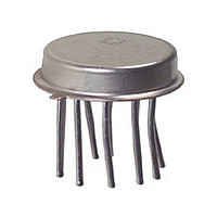
Package Type
TO-100
Lead Free Status / Rohs Status
Not Compliant
Available stocks
Company
Part Number
Manufacturer
Quantity
Price


application of Figure 2, a 10 ppm/°C input resistor used with a
100 ppm/°C capacitor may result in a maximum overall circuit
gain drift of:
Although R
perature stability, the offset circuit of resistors R4 and R5 may
also have a slight effect on the offset temperature drift of the
circuit. The offset will change with variations in the resistance of
R4 and supply voltage changes. In most applications the offset
adjustment is very small, and the offset drift attributable to this
circuit will be negligible. In the bipolar mode, however, both the
positive reference and the resistor used to offset the signal range
will have a pronounced effect on offset drift. A high quality refer-
ence and resistor should be used to minimize offset drift errors.
Other circuit components do not directly influence temperature
performance as long as their actual values are not so different
from nominal value as to preclude operation. This includes
integration capacitor C2. A change in the capacitance value of
C2 results in a different rate of voltage change across C2, but
this is compensated by an equal effect when C2 is discharged
by the switched 1 mA current source so that no net effect occurs.
The temperature effects of the components described above are
the same when the ADVFC32 is configured for negative or
bipolar input ranges, or F/V conversion.
OTHER CIRCUIT CONSIDERATIONS
The input amplifier connected to Pins 1, 13, and 14 is not a
standard operational amplifier. Although it operates like an op
amp in most applications, two key differences should be noted.
First, the bias current of the positive input is typically 40 nA
while the bias current of the inverting input is ± 8 nA. Therefore,
any attempt to cancel input offset voltage due to bias currents
by matching input resistors will create worse offsets. Second, the
output of this amplifier will sink only 1 mA, even though it will
source as much as 10 mA. When used in the F/V mode, the
amplifier must be buffered if large sink currents are required.
MICROPROCESSOR OPERATED A/D CONVERTER
With the addition of a few external components the ADVFC32
can be used as a ± 10 V A/D microprocessor front end. Although
100 ppm/°C (ADVFC32BH) + 100 ppm/°C (C1)
+ 10 ppm/°C (R
IN
and C1 have the most pronounced effect on tem-
IN
) = 210 ppm/°C
the nonlinearity of the ADVFC32 is only 0.05% maximum
(0.01% typ), the resolution is much higher, allowing it to be
used in 16-bit measurement and control systems where a mono-
tonic transfer function is essential. The resolution of the circuit
shown in Figure 5 is dependent on the amount of time allowed
to count the ADVFC32 frequency output. Using a full-scale
frequency of 100 kHz, an 8-bit conversion can be made in about
10 ms, and a 2 second time period allows a 16-bit measurement,
including offset and gain calibration cycles.
As shown in Figure 5, the input signal is selected via the AD7590
input multiplexer. Positive and negative references as well as a
ground input are provided to calibrate the A/D. This is very
important in systems subject to moderate or extreme temperature
changes since the gain temperature coefficient of the ADVFC32
is as high as ± 150 ppm/°C. By using the calibration cycles, the
A/D conversion will be as accurate as the references provided.
The AD542 following the input multiplexer provides a high
impedance input (10
from the relatively low impedance ADVFC32 input.
If higher linearity is required, the ADVFC32 can be operated at
10 kHz, but this will require a proportionately longer conversion
time. Conversely, the conversion time can be decreased at the
expense of nonlinearity by increasing the maximum frequency to
as high as 500 kHz.
HIGH NOISE IMMUNITY, HIGH CMRR ANALOG
DATA LINK
In many applications, a signal must be sensed at a remote site
and sent through a very noisy environment to a central location
for further processing. In these cases, even a shielded cable may
not protect the signal from noise pickup. The circuit of Figure 6
provides a solution in these cases. Due to the optocoupler and
voltage-to-frequency conversion, this data link is extremely
insensitive to noise and common-mode voltage interference. For
even more protection, an optical fiber link substituted for the
HCPL2630 will provide common-mode rejection of more than
several hundred kilovolts and virtually total immunity to electrical
noise. For most applications, however, the frequency modulated
signal has sufficient noise immunity without using an optical fiber
link, and the optocoupler provides common-mode isolation up
to 3000 V dc.
12
ohms) and buffers the switch resistance
ADVFC32
Related parts for ADVFC32SH/883B
Image
Part Number
Description
Manufacturer
Datasheet
Request
R

Part Number:
Description:
IC,Voltage-to-Frequency Converter,BIPOLAR,CAN,10PIN
Manufacturer:
Analog Devices Inc
Datasheet:

Part Number:
Description:
±1.7g Dual-Axis IMEMS Accelerometer Evaluation Board
Manufacturer:
Analog Devices Inc
Datasheet:

Part Number:
Description:
Inertial Sensor Evaluation System
Manufacturer:
Analog Devices Inc
Datasheet:
Part Number:
Description:
Manufacturer:
Analog Devices Inc
Datasheet:
Part Number:
Description:
Manufacturer:
Analog Devices Inc
Datasheet:
Part Number:
Description:
Manufacturer:
Analog Devices Inc
Datasheet:
Part Number:
Description:
Manufacturer:
Analog Devices Inc
Datasheet:
Part Number:
Description:
Manufacturer:
Analog Devices Inc
Datasheet:
Part Number:
Description:
Manufacturer:
Analog Devices Inc
Datasheet:
Part Number:
Description:
Manufacturer:
Analog Devices Inc
Datasheet:
Part Number:
Description:
Manufacturer:
Analog Devices Inc
Datasheet:
Part Number:
Description:
Manufacturer:
Analog Devices Inc
Datasheet:
Part Number:
Description:
Manufacturer:
Analog Devices Inc
Datasheet: