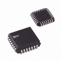
DAC8413FPC Analog Devices Inc, DAC8413FPC Datasheet - Page 16

DAC8413FPC
Manufacturer Part Number
DAC8413FPC
Description
IC DAC 12BIT QUAD READBK 28-PLCC
Manufacturer
Analog Devices Inc
Datasheet
1.DAC8412FPCZ.pdf
(20 pages)
Specifications of DAC8413FPC
Rohs Status
RoHS non-compliant
Settling Time
6µs
Number Of Bits
12
Data Interface
Parallel
Number Of Converters
4
Voltage Supply Source
Single Supply
Power Dissipation (max)
330mW
Operating Temperature
-40°C ~ 85°C
Mounting Type
Surface Mount
Package / Case
28-LCC (J-Lead)
Number Of Channels
4
Resolution
12b
Conversion Rate
167KSPS
Interface Type
Parallel
Single Supply Voltage (typ)
5V
Dual Supply Voltage (typ)
±15V
Architecture
R-2R
Power Supply Requirement
Single/Dual
Output Type
Voltage
Integral Nonlinearity Error
±4LSB
Single Supply Voltage (min)
4.75V
Single Supply Voltage (max)
5.25V
Dual Supply Voltage (min)
±14.25V
Dual Supply Voltage (max)
±15.75V
Operating Temp Range
-40C to 85C
Operating Temperature Classification
Industrial
Mounting
Surface Mount
Pin Count
28
Package Type
PLCC
Lead Free Status / Rohs Status
Not Compliant
Available stocks
Company
Part Number
Manufacturer
Quantity
Price
Company:
Part Number:
DAC8413FPC
Manufacturer:
VISHAY
Quantity:
6 652
Company:
Part Number:
DAC8413FPC
Manufacturer:
Analog Devices Inc
Quantity:
10 000
Part Number:
DAC8413FPC
Manufacturer:
ADI/亚德诺
Quantity:
20 000
Company:
Part Number:
DAC8413FPC-REEL
Manufacturer:
Analog Devices Inc
Quantity:
10 000
Company:
Part Number:
DAC8413FPCZ
Manufacturer:
Analog Devices Inc
Quantity:
10 000
Company:
Part Number:
DAC8413FPCZ-REEL
Manufacturer:
Analog Devices Inc
Quantity:
10 000
DAC8412/DAC8413
Careful attention to grounding is important for accurate
operation of the DAC8412. This is not because the DAC8412 is
more sensitive than other 12-bit DACs, but because with four
outputs and two references, there is greater potential for ground
loops. Because the DAC8412 has no analog ground, the ground
must be specified with respect to the reference.
REFERENCE CONFIGURATIONS
Output voltage ranges can be configured as either unipolar or
bipolar, and within these choices, a wide variety of options
exists. The unipolar configuration can be either positive or
negative voltage output, and the bipolar configuration can be
either symmetrical or nonsymmetrical.
INPUT
REF10
+15V
OUTPUT
TRIM
+
DB11..DB0
V
LOGIC
R/W
Figure 39. Unipolar +10 V Operation
CS
A0
A1
10kΩ
DATAOUT_DB11
+10V OPERATION
READBACK
OP400
0.2µF
V
V
REFL
REFH
DGND
DAC8412
DAC8413
–15V
+15V
V
OR
V
DD
SS
Figure 38. Simplified I/O Logic Diagram
0.1µF
//10µF
READOUTBAR
Rev. F | Page 16 of 20
READBACKDATAIN_DB11
100kΩ
Figure 40 (symmetrical bipolar operation) shows the DAC8412
configured for ±10 V operation. See the
full explanation of reference operation. Adjustments may not be
required for many applications since the AD688 is a very high
accuracy reference. However, if additional adjustments are
required, adjust the DAC8412 full scale first. Begin by loading
the digital full-scale code (0xFFF), and then adjust the gain
adjust potentiometer to attain a DAC output voltage of 9.9976 V.
Then, adjust the balance adjust to set the center-scale output
voltage to 0.000 V.
GAIN
RDDACA
WRDACA
RDDACB
WRDACB
RDDACC
WRDACC
RDDACD
WRDACD
REGISTER
INPUT
BALANCE
100kΩ
WRDB10
WRDB11
WRDB0
WRDB1
WRDB2
WRDB3
WRDB4
WRDB5
WRDB6
WRDB7
WRDB8
WRDB9
Figure 40. Symmetrical Bipolar Operation
READBACKDATAIN_DB10
AD688 FOR ±10V
READOUT
REGISTER
AD588 FOR ±5V
+15V
OUTPUT
39kΩ
V
DAC A
DAC B
DAC C
DAC D
REFH
1µF
0.2µF
0.2µF
6.2Ω
6.2Ω
V
DD
±5 OR ±10V OPERATION
AD688
V
SS
DAC8412
DAC8413
V
V
REFH
REFL
V
V
V
V
V
LDAC
RESET
+15V
–15V
OR
V
V
data sheet for a
OUTA
OUTB
OUTC
OUTD
REFL
DD
SS
0.1µF
//10µF


