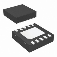
DAC122S085CISDX/NOPB National Semiconductor, DAC122S085CISDX/NOPB Datasheet - Page 3

DAC122S085CISDX/NOPB
Manufacturer Part Number
DAC122S085CISDX/NOPB
Description
DAC 12BIT DUAL R-R 10-LLP
Manufacturer
National Semiconductor
Series
PowerWise®r
Datasheet
1.DAC122S085CIMMNOPB.pdf
(20 pages)
Specifications of DAC122S085CISDX/NOPB
Settling Time
6µs
Number Of Bits
12
Data Interface
Serial
Number Of Converters
2
Voltage Supply Source
Single Supply
Power Dissipation (max)
2.3mW
Operating Temperature
-40°C ~ 105°C
Mounting Type
Surface Mount
Package / Case
10-LLP
For Use With
DAC122S085EB - BOARD EVALUATION DAC122S085
Lead Free Status / RoHS Status
Lead free / RoHS Compliant
Other names
DAC122S085CISDX
Pin Descriptions
Pin No.
MSOP
LLP
10
11
1
2
3
4
5
6
7
8
9
(LLP only)
Symbol
V
SYNC
V
V
SCLK
GND
PAD
NC
NC
REFIN
D
OUTA
OUTB
V
IN
A
Analog Output
Analog Output
Analog Input
Digital Input
Digital Input
Digital Input
Ground
Ground
Supply
Type
Power supply input. Must be decoupled to GND.
Channel A Analog Output Voltage.
Channel B Analog Output Voltage.
Not Connected
Not Connected
Ground reference for all on-chip circuitry.
Unbuffered reference voltage shared by both channels. Must be
decoupled to GND.
Serial Data Input. Data is clocked into the 16-bit shift register on the falling
edges of SCLK after the fall of SYNC.
Frame synchronization input for the data input. When this pin goes low,
it enables the input shift register and data is transferred on the falling
edges of SCLK. The DAC is updated on the 16th clock cycle unless
SYNC is brought high before the 16th clock, in which case the rising edge
of SYNC acts as an interrupt and the write sequence is ignored by the
DAC.
Serial Clock Input. Data is clocked into the input shift register on the
falling edges of this pin.
Exposed die attach pad can be connected to ground or left floating.
Soldering the pad to the PCB offers optimal thermal performance and
enhances package self-alignment during reflow.
3
Description
www.national.com


