DS4402N+T&R Maxim Integrated Products, DS4402N+T&R Datasheet - Page 2
DS4402N+T&R
Manufacturer Part Number
DS4402N+T&R
Description
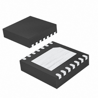
IC DAC 2CH I2C ADJ 14-TDFN
Manufacturer
Maxim Integrated Products
Datasheet
1.DS4402NTR.pdf
(9 pages)
Specifications of DS4402N+T&R
Number Of Bits
5
Data Interface
I²C, Serial
Number Of Converters
2
Voltage Supply Source
Single Supply
Operating Temperature
-40°C ~ 85°C
Mounting Type
Surface Mount
Package / Case
14-TDFN Exposed Pad
Lead Free Status / RoHS Status
Lead free / RoHS Compliant
Power Dissipation (max)
-
Settling Time
-


ABSOLUTE MAXIMUM RATINGS
Voltage Range on V
Voltage Range on A0, A1, FS0, FS1, FS2, FS3,
Two/Four-Channel, I
OUTPUT CURRENT CHARACTERISTICS
(V
Stresses beyond those listed under “Absolute Maximum Ratings” may cause permanent damage to the device. These are stress ratings only, and functional
operation of the device at these or any other conditions beyond those indicated in the operational sections of the specifications is not implied. Exposure to
absolute maximum rating conditions for extended periods may affect device reliability.
RECOMMENDED OPERATING CONDITIONS
(T
DC ELECTRICAL CHARACTERISTICS
(V
2
Supply Current
Input Leakage (SDA, SCL)
Output Leakage (SDA)
Output Current Low (SDA)
Address Input Resistors
Reference Voltage
I/O Capacitance
Supply Voltage
Input Logic 1 (SDA, SCL, A0, A1)
Input Logic 0 (SDA, SCL, A0, A1)
Output Voltage for Sinking Current
Output Voltage for Sourcing
Current
Full-Scale Sink Output Current
Full-Scale Source Output Current
Output-Current Full-Scale
Accuracy
Output-Current Temperature Drift
A
CC
CC
Relative to Ground.............................................-0.5V to +6.0V
OUT0, OUT1, OUT2, and OUT3 Relative to
Ground ................-0.5V to (V
= -40°C to +85°C.)
______________________________________________________________________
= +2.7V to +5.5V, T A = -40°C to +85°C.)
= +2.7V to +5.5V, T
PARAMETER
PARAMETER
PARAMETER
CC
, SDA, and SCL
A
= -40°C to +85°C.)
CC
+ 0.5V) (Not to exceed 6.0V.)
SYMBOL
SYMBOL
V
I
OUT:SOURCE
OUT:SOURCE
V
V
SYMBOL
I
C
V
R
OUT:SINK
I
I
V
V
OUT:SINK
I
I
CC
I
REF
I
OL
I/O
OUT:TC
CC
IL
OUT:FS
L
IN
IH
IL
(Note 1)
V
(Note 2)
V
V
V
CC
CC
OL
OL
= 5.5V
= 5.5V
= 0.4V
= 0.6V
(Note 3)
(Note 3)
(Note 3)
(Note 3)
+25°C, V
resistor; V
V
(Note 4)
OUT:SOURCE
2
C Adjustable Current DAC
CC
DS4402
DS4404
OUT:SINK
CONDITIONS
CONDITIONS
= 4.0V; using ideal R
CONDITIONS
= V
Operating Temperature Range ...........................-40°C to +85°C
Storage Temperature Range .............................-55°C to +125°C
Soldering Temperature .....................................Refer to IPC/JEDEC
CC
= 0.5V;
- 0.8V
FS
0.7 x V
MIN
MIN
MIN
-2.0
-0.3
0.5
0.5
2.7
3
6
0
CC
TYP
1.23
TYP
TYP
240
2.5
70
J-STD-020 Specification
V
0.3 x V
CC
MAX
MAX
V
MAX
500
500
V
-0.5
+ 0.3
0.5
2.0
5.0
5.5
10
CC
1
1
CC
CC
-
ppm/°C
UNITS
UNITS
UNITS
mA
mA
mA
μA
μA
μA
k
pF
%
V
V
V
V
V
V
Related parts for DS4402N+T&R
Image
Part Number
Description
Manufacturer
Datasheet
Request
R

Part Number:
Description:
DAC (D/A Converters) IC DAC 2CH I2C ADJ justable Sink-Source
Manufacturer:
Maxim Integrated Products
Datasheet:

Part Number:
Description:
Two/Four-Channel, I2C Adjustable Current DAC
Manufacturer:
MAXIM [Maxim Integrated Products]
Datasheet:

Part Number:
Description:
MAX7528KCWPMaxim Integrated Products [CMOS Dual 8-Bit Buffered Multiplying DACs]
Manufacturer:
Maxim Integrated Products
Datasheet:
Part Number:
Description:
Single +5V, fully integrated, 1.25Gbps laser diode driver.
Manufacturer:
Maxim Integrated Products
Datasheet:
Part Number:
Description:
Single +5V, fully integrated, 155Mbps laser diode driver.
Manufacturer:
Maxim Integrated Products
Datasheet:
Part Number:
Description:
VRD11/VRD10, K8 Rev F 2/3/4-Phase PWM Controllers with Integrated Dual MOSFET Drivers
Manufacturer:
Maxim Integrated Products
Datasheet:
Part Number:
Description:
Highly Integrated Level 2 SMBus Battery Chargers
Manufacturer:
Maxim Integrated Products
Datasheet:
Part Number:
Description:
Current Monitor and Accumulator with Integrated Sense Resistor; ; Temperature Range: -40°C to +85°C
Manufacturer:
Maxim Integrated Products
Part Number:
Description:
TSSOP 14/A°/RS-485 Transceivers with Integrated 100O/120O Termination Resis
Manufacturer:
Maxim Integrated Products
Part Number:
Description:
TSSOP 14/A°/RS-485 Transceivers with Integrated 100O/120O Termination Resis
Manufacturer:
Maxim Integrated Products
Part Number:
Description:
QFN 16/A°/AC-DC and DC-DC Peak-Current-Mode Converters with Integrated Step
Manufacturer:
Maxim Integrated Products
Part Number:
Description:
TDFN/A/65V, 1A, 600KHZ, SYNCHRONOUS STEP-DOWN REGULATOR WITH INTEGRATED SWI
Manufacturer:
Maxim Integrated Products
Part Number:
Description:
Integrated Temperature Controller f
Manufacturer:
Maxim Integrated Products
Part Number:
Description:
SOT23-6/I°/45MHz to 650MHz, Integrated IF VCOs with Differential Output
Manufacturer:
Maxim Integrated Products
Part Number:
Description:
SOT23-6/I°/45MHz to 650MHz, Integrated IF VCOs with Differential Output
Manufacturer:
Maxim Integrated Products