RoHS Compliant. See ordering information)
Lead Free Finish/RoHS Compliant (Note1) ("P" Suffix designates
Epoxy meets UL 94 V-0 flammability rating
Moisure Sensitivity Level 1
Notes: 1. High Temperature Solder Exemption Applied, see EU Directive Annex Notes 7.
Micro Commercial Components
use in low-speed switching and general purpose.
Silicon NPN medium power Darlington transistors in a plastic envelope, primarily for
SYMBOL
I
I
V
V
V
h
h
f
C
t
t
t
GENERAL DESCRIPTION
QUICK REFERENCE DATA
LIMITING VALUES
ELECTRICAL CHARACTERISTICS
Revision: A
CBO
EBO
T
ON
S
F
SYMBOL
V
V
I
I
P
V
I
V
t
V
V
V
I
I
I
P
T
T
FE1
FE2
C
CM
csat
f
C
B
BM
(BR)CEO
CEsat1
CEsat2
C
SYMBOL
stg
j
CESM
CEO
TOT
CEsat
BE
CESM
CEO
EBO
TOT
M C C
Collector-base cut-off current
Emitter-base cut-off current
Collector-emitter breakdown voltage
Collector-emitter saturation voltage
Collector-emitter saturation voltage
DC current gain
DC current gain
Transition frequency at f=1MHz
Collector capacitance at f=1MHz
On times
Turn-off storage time
Fall time
Collector-emitter voltage peak value
Collector-emitter voltage (open base )
Collector current (DC)
Collector current peak value
Total power dissipation
Collector -emitter saturation voltage
Collector saturation current
Emitter forward voltage
Fall time
Collector-emitter voltage peak value
Collector-emitter voltage (open base)
Emitter-base voltage (open collector)
Collector current (DC)
Base current(DC)
Base current peak value
Total power dissipation
Storage temperature
Junction temperature
PARAMETER
PARAMETER
PARAMETER
TM
www.mccsemi.com
���������� ���
���omponents
20736 Marilla Street Chatsworth
��������
���� ������ �!��"#���
$
%�� � � ���� �!��"#���
V
T
V
V
I
I
I
I
I
I
V
I
V
I
V
I
V
V
T
I
I
I
I
I
V
CONDITIONS
mb
C
C
C
C
C
C
C
C
C
C
B
E
C
B1
BE
CONDITION
BE
mb
CB
EB
=100mA
=3.0A,I
=8A,I
=3A,V
=8A,V
=0.5A,V
CB
=3A,I
CC
=3A,I
CC
=3A,I
CC
=8A;
=0.08A
=8A
=3.0A;
CC
<=25
=-I
=0V
CONDITION
=100V
=10V
=30V
=30V
=30V
<=25
=0V
=30V
=5V
B2
B
B
B
B
o
=0.3A;
C
=80mA
CE
CE
=0.3A,
=0.3A,
=0.3A,
o
B
C
=4V
=4V
=12mA
CE
=4V
MIN
100
MIN
-60
-60
100
8.0
16
75
1000
MIN
100
100
MAX
MAX
150
150
20000
4.0
75
100
100
MAX UNIT
5
0.12
8
2.0
2.0
4.0
20
1 of 2
UNIT
UNIT
A
us
MHz
V
A
W
V
V
mA
A
W
o
o
A
V
V
V
A
A
uA
pF
us
us
V
C
C
us
V
V
V
Darlington Transistor
F
A
K
G
H
K
S
DIM
J
L
N
Q
R
T
U
A
B
C
D
F
V
H
L
G
Silicon Power
.012
.190
.500
.045
.190
.045
.230
.380
.020
.139
.100
.080
.045
.560
.140
-----
1
---
MIN
INCHES
2N6045
N
2
B
3
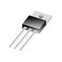
TO-220
MAX
.025
.580
.055
.161
.110
.060
.210
.135
.115
.270
.625
.420
.190
.045
.050
.250
-----
NPN
V
DIMENSIONS
D
Q
PIN 1.
PIN 2.
PIN 3.
12.70
14.22
0.30
1.14
3.53
2.29
1.14
4.83
2.04
5.84
9.65
3.56
0.51
2.54
1.15
-----
MIN
---
U
MM
BASE
COLLECTOR
EMITTER
T
J
14.73
15.88
10.67
MAX
6.35
2.79
0.64
1.52
5.33
1.39
1.14
4.09
3.43
2.92
6.86
4.82
1.27
-----
2011/01/01
C
NOTE
S
R