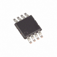
MAX5302CUA Maxim Integrated Products, MAX5302CUA Datasheet

MAX5302CUA
Specifications of MAX5302CUA
Available stocks
Related parts for MAX5302CUA
MAX5302CUA Summary of contents
Page 1
... Single-Supply Operation o Low Supply Current: 0.28mA Normal Operation o Available in 8-Pin µMAX o Power-On Reset Clears DAC Output to Zero o SPI/QSPI/MICROWIRE Compatible o Schmitt-Trigger Digital Inputs for Direct Optocoupler Interface PART Applications MAX5302CUA MAX5302EUA TOP VIEW FB OUT MAX5302 Features 2µA Shutdown Mode Ordering Information TEMP ...
Page 2
... Input Voltage Low V Input Leakage Current I IN Input Capacitance C 2 _______________________________________________________________________________________ Operating Temperature Ranges + 0.3V) MAX5302CUA ...................................................0°C to +70°C DD MAX5302EUA ................................................-40°C to +85°C Junction Temperature ......................................................+150°C Storage Temperature Range .............................-65°C to +150°C Lead Temperature (soldering, 10sec) .............................+300°C = +2.5V 5kΩ 100pF ...
Page 3
Low-Power, 12-Bit Voltage-Output DAC ELECTRICAL CHARACTERISTICS (continued) (Circuit of Figure +5V ±10 ues are +25°C. Output buffer connected in unity-gain configuration.) A PARAMETER SYMBOL DIGITAL INPUTS DYNAMIC PERFORMANCE Voltage Output Slew Rate ...
Page 4
Low-Power, 12-Bit Voltage-Output DAC with Serial Interface __________________________________________Typical Operating Characteristics (V = +5V 5kΩ 100pF +25°C, unless otherwise noted INTEGRAL NONLINEARITY vs. REFERENCE VOLTAGE 0.3 0.2 0.1 0 -0.1 -0.2 ...
Page 5
Low-Power, 12-Bit Voltage-Output DAC (V = +5V 5kΩ 100pF MAJOR-CARRY TRANSITION CS 5V/div OUT AC-COUPLED 100mV/div 10µs/div _______________________________________________________________________________________ with Serial Interface Typical Operating Characteristics (continued) = +25°C, unless otherwise noted.) SCLK ...
Page 6
Low-Power, 12-Bit Voltage-Output DAC with Serial Interface _____________________Pin Description PIN NAME FUNCTION 1 OUT DAC Output Voltage CS 2 Chip-Select Input. Active low. 3 DIN Serial-Data Input 4 SCLK Serial-Clock Input 5 FB DAC Output Amplifier Feedback 6 REF Reference ...
Page 7
Low-Power, 12-Bit Voltage-Output DAC SCLK MAX5302 DIN CS Figure 2. Connections for MICROWIRE DIN MAX5302 SCLK CS CPOL = 0, CPHA = 0 Figure 3. Connections for SPI/QSPI Table 1. Serial-Interface Programming Commands 16-BIT SERIAL WORD D11............... ...
Page 8
Low-Power, 12-Bit Voltage-Output DAC with Serial Interface CS SCLK 1 DIN D11 D10 Figure 5. Serial-Interface Timing Diagram CS t CSS t CSO SCLK DIN Figure 6. Detailed Serial-Interface Timing Diagram DIN SCLK ...
Page 9
Low-Power, 12-Bit Voltage-Output DAC bits (C2, C1, C0), followed by the 12+1 data bits D11...D0, S0 (Figure 4). Set the sub-bit (S0) to zero. The 3-bit control code determines the register to be updated and the configuration when exiting shutdown. ...
Page 10
Low-Power, 12-Bit Voltage-Output DAC with Serial Interface +5V REF V DD MAX5302 DAC GND Figure 9. Unipolar Rail-to-Rail Output Circuit Digitally Programmable Current Source The circuit of Figure 12 places an NPN transistor (2N3904 or similar) within the op amp ...
Page 11
Low-Power, 12-Bit Voltage-Output DAC +5V +5V MAX495 26k AC REFERENCE INPUT 10k 500mVp-p REF DAC Figure 11. AC Reference Input Circuit Chip Information TRANSISTOR COUNT: 3053 SUBSTRATE CONNECTED TO AGND ______________________________________________________________________________________ with Serial Interface V DD OUT MAX5302 GND Figure ...
Page 12
... Maxim cannot assume responsibility for use of any circuitry other than circuitry entirely embodied in a Maxim product. No circuit patent licenses are implied. Maxim reserves the right to change the circuitry and specifications without notice at any time. 12 ____________________Maxim Integrated Products, 120 San Gabriel Drive, Sunnyvale, CA 94086 408-737-7600 © 1999 Maxim Integrated Products Printed USA is a registered trademark of Maxim Integrated Products ...


