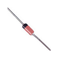
1N5221BTA2 ON Semiconductor, 1N5221BTA2 Datasheet - Page 2

1N5221BTA2
Manufacturer Part Number
1N5221BTA2
Description
Manufacturer
ON Semiconductor
Type
Voltage Regulatorr
Datasheet
1.1N5221BTA2.pdf
(12 pages)
Specifications of 1N5221BTA2
Number Of Elements
Single
Package Type
DO-35
Zener Voltage (typ)
2.4V
Voltage Tolerance
5%
Knee Impedance
30Ohm
Operating Temperature Classification
Military
Rev Curr
100uA
Mounting
Through Hole
Pin Count
2
Operating Temp Range
-65C to 200C
Lead Free Status / Rohs Status
Not Compliant
2. TOLERANCE
3. ZENER VOLTAGE (V
4. ZENER IMPEDANCE (Z
5. TEMPERATURE COEFFICIENT (q
* For more information on special selections contact your nearest ON Semiconductor representative.
ELECTRICAL CHARACTERISTICS
otherwise noted, Based on dc measurements at thermal
equilibrium; lead length = 3/8 ; thermal resistance of heat sink
= 30 C/W, V
ELECTRICAL CHARACTERISTICS
length = 3/8 ; thermal resistance of heat sink = 30 C/W, V
Symbol
1N5221B
1N5222B
1N5223B
1N5224B
1N5225B
1N5226B
1N5227B
1N5228B
1N5229B
1N5230B
1N5231B
1N5232B
1N5233B
1N5234B
1N5235B
(Note 2.)
Device
Device
The JEDEC type numbers shown indicate a tolerance of 5%.
The zener voltage is measured with the device junction in the thermal equilibrium at the lead temperature (T
length.
Z
0.1 I
Test conditions for temperature coefficient are as follows:
Device to be temperature stabilized with current applied prior to reading breakdown voltage at the specified ambient temperature.
Z
Z
q
I
I
V
V
V
ZK
I
I
ZT
ZT
VZ
ZT
ZK
R
F
A. I
B. I
R
Z
F
and Z
Z(dc)
ZT
ZT
= 7.5 mA, T
= Rated I
F
with the ac frequency = 60 Hz.
ZK
Reverse Zener Voltage @ I
Reverse Current
Maximum Zener Impedance @ I
Reverse Current
Maximum Zener Impedance @ I
Reverse Leakage Current @ V
Breakdown Voltage
Forward Current
Forward Voltage @ I
Maximum Zener Voltage Temperature Coefficient
= 1.1 V Max @ I
1N5226B
1N5228B
1N5231B
1N5232B
1N5234B
1N5235B
1N5221B
1N5222B
1N5223B
1N5224B
1N5225B
1N5227B
1N5229B
1N5230B
1N5233B
Marking
are measured by dividing the ac voltage drop across the device by the ac current applied. The specified limits are for I
Device
Device
ZT
, T
1
Z
= 25 C, T
) MEASUREMENT
1
Z
= 25 C, T
) DERIVATION
2.375
2.565
2.28
2.66
2.85
3.14
3.42
3.71
4.09
4.47
4.85
5.32
5.89
6.46
Min
5.7
F
Parameter
= 200 mA for all types)
F
Zener Voltage (Note 3.)
2
V
= 125 C (1N5221B through 1N5242B)
2
Z
VZ
= 125 C (1N5243B through 1N5281B)
Nom
(Volts)
2.4
2.5
2.7
2.8
3.0
3.3
3.6
3.9
4.3
4.7
5.1
5.6
6.0
6.2
6.8
ZT
) *
(T
(T
A
A
R
= 25 C unless
ZT
ZK
= 25 C unless otherwise noted, Based on dc measurements at thermal equilibrium; lead
2.625
2.835
Max
2.52
2.94
3.15
3.46
3.78
4.09
4.51
4.93
5.35
5.88
6.51
7.14
6.3
1N5221B Series
F
http://onsemi.com
@ I
= 1.1 V Max @ I
mA
20
20
20
20
20
20
20
20
20
20
20
20
20
20
20
ZT
2
Z
Zener Impedance (Note 4.)
ZT
30
30
30
30
29
28
24
23
22
19
17
11
W
@ I
7
7
5
F
= 200 mA for all types)
ZT
1200
1250
1300
1400
1600
1600
1700
1900
2000
1900
1600
1600
1600
1000
V
750
W
Z
Z
ZK
V
R
Zener Voltage Regulator
@ I
ZK
0.25
0.25
0.25
0.25
0.25
0.25
0.25
0.25
0.25
0.25
0.25
0.25
0.25
0.25
0.25
mA
I
F
Leakage Current
I
I
I
100
100
R
ZT
75
75
50
25
15
10
5
5
5
5
5
5
3
A
L
V
) at 30 C
I
R
F
@ V
R
Volts
3.5
1
1
1
1
1
1
1
1
1
2
2
3
4
5
1 C and 3/8 lead
(Note 5.)
–0.085
–0.085
–0.075
–0.065
–0.08
–0.08
–0.07
–0.06
+ 0.03
0.038
0.038
0.045
V
%/5C
0.055
0.05
q
q
0.03
VZ
VZ
Z(ac)
=


