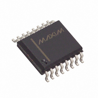
MAX510BCWE Maxim Integrated Products, MAX510BCWE Datasheet

MAX510BCWE
Specifications of MAX510BCWE
Available stocks
Related parts for MAX510BCWE
MAX510BCWE Summary of contents
Page 1
... REFC Functional Diagrams continued at end of data sheet MICROWIRE is a trademark of National Semiconductor Corp. SPI and QSPI are trademarks of Motorola. ________________________________________________________________ Maxim Integrated Products For pricing, delivery, and ordering information, please contact Maxim Direct at 1-888-629-4642, or visit Maxim’s website at www.maxim-ic.com. Quad, Serial 8-Bit DACs ...
Page 2
Quad, Serial 8-Bit DACs with Rail-to-Rail Outputs ABSOLUTE MAXIMUM RATINGS V to DGND ..............................................................-0.3V, + AGND...............................................................-0.3V, + DGND ...............................................................-6V, +0. AGND ...............................................................-6V, +0. .................................................................-0.3V, +12V DD SS ...
Page 3
ELECTRICAL CHARACTERISTICS (continued +5V ±10 -5.5V, V REF = 4V, AGND = DGND = 0V 10kΩ 100pF MIN to T MAX , ...
Page 4
Quad, Serial 8-Bit DACs with Rail-to-Rail Outputs ELECTRICAL CHARACTERISTICS (continued +5V ±10 -5.5V, V REF = 4V, AGND = DGND = 0V 10kΩ 100pF ...
Page 5
Operating Characteristics (T = +25°C, unless otherwise noted.) A OUTPUT SINK CURRENT vs OUT VREF = + GND = 0V SS ALL DIGITAL ...
Page 6
Quad, Serial 8-DACs with Rail-to-Rail Outputs ____________________________Typical Operating Characteristics (continued +25°C, unless otherwise noted.) A ZERO-CODE ERROR vs. NEGATIVE SUPPLY VOLTAGE 5 +5V DD 4.8 VREF = +4V 4.6 4.4 4.2 4.0 3.8 3.6 3.4 0 ...
Page 7
Operating Characteristics (continued +25°C, unless otherwise noted.) A CLOCK FEEDTHROUGH A = SCLK, 333kHz B = OUT_, 10mV/div TIMEBASE = 2μs/div NEGATIVE SETTLING TIME (V = AGND 100mV A = DIGITAL INPUT, 5V/div B = ...
Page 8
Quad, Serial 8-Bit DACs with Rail-to-Rail Outputs ______________________________________________________________Pin Description PIN NAME MAX509 MAX510 1 1 OUTB 2 2 OUTA – REFB – 4 REFAB 5 – REFA 6 5 AGND 7, 14 – N.C. 8 ...
Page 9
Description At power-on, the serial interface and all DACs are cleared and set to code zero. The serial data output (DOUT) is set to transition on SCLK's rising edge. The MAX509/MAX510 communicate with microproces- sors through a synchronous, full-duplex, ...
Page 10
Quad, Serial 8-Bit DACs with Rail-to-Rail Outputs CS t CSS t CSH0 SCLK t DS DIN DOUT LDAC NOTE: TIMING SPECIFICATION t IS RECOMMENDED TO MINIMIZE OUTPUT GLITCH, BUT IS NOT MANDATORY. CLL Figure 2. Detailed Serial Interface Timing (Mode ...
Page 11
Serial Input Data Format and Control Codes The 12-bit serial input format shown in Figure 3 com- prises two DAC address bits (A1, A0), two control bits (C1, C0) and eight bits of data (D0...D7). The 4-bit address/control code configures ...
Page 12
Quad, Serial 8-Bit DACs with Rail-to-Rail Outputs Set DOUT Phase – SCLK Falling (Mode (LDAC = x) This command resets DOUT to transition at ...
Page 13
MAX509 SCLK SCLK MAX510 DIN DOUT DIN CS CS MAX509 SCLK SCLK MAX510 DIN DIN CS CS Figure 6. Daisy-chained or individual MAX509/MAX510s are simultaneously updated by bringing CS high. Only three wires are required. DIN SCLK LDAC CS1 CS2 ...
Page 14
Quad, Serial 8-Bit DACs with Rail-to-Rail Outputs REF_ AGND SHOWN FOR ALL 1 ON DAC Figure 8. DAC Simplified Circuit Diagram If multiple devices share a common DIN line, Figure ...
Page 15
SYSTEM GND OUTC OUTD V DD REFC REFD Figure 9. Suggested MAX509 PC Board Layout for Minimizing Crosstalk (Bottom View) Unipolar-Output, 2-Quadrant Multiplication In unipolar operation, the output voltages and the refer- ence input(s) are the same polarity. Figures 11 ...
Page 16
Quad, Serial 8-Bit DACs with Rail-to-Rail Outputs REFERENCE INPUTS ( REFA REFB REFC REFD DAC A DAC B SERIAL INTERFACE NOT SHOWN DAC C DAC D V AGND ...
Page 17
SERIAL INTERFACE NOT SHOWN 0.1μF R1 330k 0.1% MAX873 +2.5V ICL7611A Figure 14. MAX509 AGND Bias Circuit (Negative Offset) 4-Quadrant Multiplication Each DAC output may be configured for 4-quadrant multiplication using Figure 16 and 17's circuit. One op amp ...
Page 18
Quad, Serial 8-Bit DACs with Rail-to-Rail Outputs +5V SERIAL INTERFACE 0.1μF NOT SHOWN 2 R1 330k 0.1% 6 MAX873 +2.5V 4 ICL7611A Figure 15. MAX510 AGND Bias Circuit (Negative Offset) REFERENCE INPUTS ( DAC A ...
Page 19
REFERENCE INPUTS 4 13 DAC A SERIAL DAC B INTERFACE NOT SHOWN DAC C DAC 0.1μF AGND OR -5V Figure 17. MAX510 Bipolar Output Circuit __Functional Diagrams (continued) CLR DGND V AGND V REFAB DOUT LDAC ...
Page 20
... MAX509BMJP -55°C to +125°C 20 CERDIP** MAX510ACPE+ 0°C to +70°C 16 PDIP MAX510BCPE+ 0°C to +70°C 16 PDIP MAX510ACWE+ 0°C to +70°C 16 Wide SO MAX510BCWE+ 0°C to +70°C 16 Wide SO MAX510AEPE+ -40°C to +85°C 16 PDIP MAX510BEPE+ -40°C to +85°C 16 PDIP MAX510AEWE+ -40°C to +85°C 16 Wide SO MAX510BEWE+ -40° ...
Page 21
... Maxim cannot assume responsibility for use of any circuitry other than circuitry entirely embodied in a Maxim product. No circuit patent licenses are implied. Maxim reserves the right to change the circuitry and specifications without notice at any time. Maxim Integrated Products, 120 San Gabriel Drive, Sunnyvale, CA 94086 408-737-7600 ____________________ 21 © 2010 Maxim Integrated Products ...
Page 22
... MAX509BMJP -55°C to +125°C 20 CERDIP** MAX510ACPE+ 0°C to +70°C 16 PDIP MAX510BCPE+ 0°C to +70°C 16 PDIP MAX510ACWE+ 0°C to +70°C 16 Wide SO MAX510BCWE+ 0°C to +70°C 16 Wide SO MAX510AEPE+ -40°C to +85°C 16 PDIP MAX510BEPE+ -40°C to +85°C 16 PDIP MAX510AEWE+ -40°C to +85°C 16 Wide SO MAX510BEWE+ -40° ...


