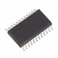
MX7847JR Maxim Integrated Products, MX7847JR Datasheet - Page 5

MX7847JR
Manufacturer Part Number
MX7847JR
Description
IC DAC 12BIT DUAL MULT 24SOIC
Manufacturer
Maxim Integrated Products
Datasheet
1.MX7847JR.pdf
(12 pages)
Specifications of MX7847JR
Settling Time
4µs
Number Of Bits
12
Data Interface
Parallel
Number Of Converters
2
Voltage Supply Source
Dual ±
Power Dissipation (max)
941mW
Operating Temperature
0°C ~ 70°C
Mounting Type
Surface Mount
Package / Case
24-SOIC (7.5mm Width)
Lead Free Status / RoHS Status
Contains lead / RoHS non-compliant
Available stocks
Company
Part Number
Manufacturer
Quantity
Price
Part Number:
MX7847JR
Manufacturer:
MAXIM/美信
Quantity:
20 000
(T
______________________________________________________________Pin Description
MX7837
____________________________Typical Operating Characteristics (continued)
A
AGNDA
17-20
21-24
= +25°C, V
10
11
12
13
14
15
16
1
2
3
4
5
6
7
8
9
–
–
–
–
PIN
A = V
TIMEBASE = 2 s/div
V
REFA
MX7847
14-24
OUTA
DD
10
11
12
13
= ±100mV SQUARE WAVE
–
1
–
2
3
4
5
6
7
8
9
–
–
–
–
–
–
SMALL-SIGNAL PULSE RESPONSE
= 15V, V
, 50mV/div
_______________________________________________________________________________________
DB3/DB11-
DB10-DB0
DB7-DB4
DB0/DB8
SS
AGNDA
AGNDB
NAME
V
V
DGND
V
V
LDAC
DB11
R
R
CSA
CSB
V
OUTA
V
OUTB
WR
= -15V, R
REFA
REFB
CS
A1
A0
FBA
FBB
DD
SS
L
= 2k , C
Chip Select – active-low logic input
Chip-Select Input for DAC A – active-low logic input
Amplifier Feedback Resistor for DAC A
Chip-Select Input for DAC B – active-low logic input
Reference Input Voltage for DAC A
Analog Output Voltage from DAC A
Analog Ground for DAC A
Positive Power Supply
Negative Power Supply
Analog Ground for DAC B
Analog Output Voltage from DAC B
Reference Input Voltage for DAC B
Digital Ground
Amplifier Feedback Resistor for DAC B
Data Bit 11 (MSB)
Write Input – active-low logic input (MX7837); positive-edge-triggered input used with
CSA and CSB (MX7847)
Asynchronous Load – DAC input, active-low
Data Bit 10 to Data Bit 0 (LSB)
Address Input – most significant address input for input latches
Address Input – least significant address input for input latches
Data Bit 7 to Data Bit 4
Data Bit 3 to Data Bit 0 (LSB), or Data Bit 11 (MSB) to Data Bit 8
L
= 100pF, unless otherwise noted.)
A
AGNDA
Complete, Dual, 12-Bit
A = V
TIMEBASE = 2 s/div
V
REFA
OUTA
FUNCTION
= ±10V SQUARE WAVE
LARGE-SIGNAL PULSE RESPONSE
, 5V/div
Multiplying DACs
A
5


