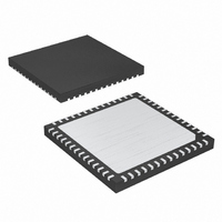
MAX5732AUTN+T Maxim Integrated Products, MAX5732AUTN+T Datasheet - Page 9

MAX5732AUTN+T
Manufacturer Part Number
MAX5732AUTN+T
Description
IC DAC 16BIT 32CHAN SER 56-TQFN
Manufacturer
Maxim Integrated Products
Datasheet
1.MAX5732BUTNT.pdf
(28 pages)
Specifications of MAX5732AUTN+T
Settling Time
20µs
Number Of Bits
16
Data Interface
MICROWIRE™, QSPI™, Serial, SPI™
Number Of Converters
32
Voltage Supply Source
Analog and Digital
Power Dissipation (max)
2.5W
Operating Temperature
0°C ~ 85°C
Mounting Type
Surface Mount
Package / Case
56-TQFN
Lead Free Status / RoHS Status
Lead free / RoHS Compliant
ELECTRICAL CHARACTERISTICS—MAX5735 (-5V to +5V Output Voltage Range) (continued)
(AV
program the offset DAC to 8000hex. V
noted. Typical values are at T
Note 1: AV
Note 2: Linearity guaranteed from code 2047 to full scale and from (V
Note 3: DNL guaranteed over all codes for (V
Note 4: Zero-scale error is measured at code 0. Full-scale error is measured at code FFFFhex.
Note 5: DC crosstalk is the change in the output level of one DAC at zero or full scale in response to the full-scale output change of all
Note 6: Digital feedthrough is a measure of the impulse injected into the analog outputs from the digital control inputs when the
Note 7: Digital crosstalk is the glitch impulse transferred to the output of one DAC at midscale while a full-scale code change is written
Note 8: DAC-to-DAC crosstalk is the glitch impulse that appears at the output of one converter due to both the digital change and
DIGITAL INPUTS (CS, SCLK, DIN, LDAC, CLR, DSP)
Input-Voltage High
Input-Voltage Low
Input Capacitance
Input Current
POWER REQUIREMENTS (AV
Output-Amplifier Positive Supply
Voltage
Output-Amplifier Negative Supply
Voltage
Output-Amplifier Supply Voltage
Difference
Analog Supply Voltage
Digital Supply Voltage
Analog Supply Current
Digital Supply Current
Output-Amplifier Positive Supply
Current
Output-Amplifier Negative Supply
Current
Power-Supply Rejection Ratio
CC
= +5.25V to +5.5V, AV
the MAX5732.
other DACs.
device is not being written to. It is measured with a worst-case change on the digital inputs.
into another DAC.
subsequent analog output change at another converter.
PARAMETER
CC
should be at least 0.25V higher than the maximum output voltage required from the DAC. Full-scale output is 5V for
_______________________________________________________________________________________
A
DD
= +25°C.)
CC
= +5V ±5%, DV
, V
32-Channel, 16-Bit, Voltage-Output
SYMBOL
SS
REF
DV
PSRR
AV
AV
DI
AI
AI
V
C
V
, AGND, AV
V
I
I
SS
IN
SS
DD
CC
IH
IN
DD
IL
CC
DD
DD
= +3.0V, R
SS
DV
DV
Digital inputs = 0 or DV
(Note 1)
AV
V
Software shutdown
V
V
V
Software shutdown
V
+ 0.3V) to (AV
DD
OUT0
IH
IH
OUT0
SS
CC
DD
DD
DD
= DV
= +2.4V, V
= +2.7V to AV
= -0.5V
L
- V
= +2.7V to +3.6V
= +4.75V to 5.25V
, DV
through V
through V
= ∞, C
SS
DD
DACs with Serial Interface
DD
, V
, DGND)
L
IL
CC
IL
CONDITIONS
= 50pF referenced to ground, T
= 0, f
OUT31
= +0.8V, f
OUT31
- 0.3V).
V
Software shutdown
DD
OUT0
, V
SS
SCLK
DD
= 0
= 0
SS
+ 0.3V) to (AV
through V
SCLK
= -5.25V to -5.5V, AGND = DGND = REFGND = GS = 0,
= 20MHz
= 20MHz
OUT31
CC
= 0
- 0.3V).
DV
-5.50
0.7 ×
A
MIN
4.75
4.75
2.70
2.4
= T
DD
MIN
TYP
to T
2.5
-20
-95
10
10
10
20
-4
5
4
MAX
, unless otherwise
-4.75
MAX
5.50
5.25
5.25
-10
0.8
3.5
6.5
±1
11
15
10
UNITS
mA
mA
mA
mA
dB
pF
µA
µA
µA
µA
V
V
V
V
V
V
V
9


