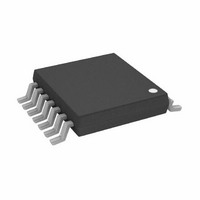
AD8303JRU-REEL Analog Devices Inc, AD8303JRU-REEL Datasheet

AD8303JRU-REEL
Specifications of AD8303JRU-REEL
Related parts for AD8303JRU-REEL
AD8303JRU-REEL Summary of contents
Page 1
FEATURES Complete Dual 12-Bit DAC Pretrimmed Internal Voltage Reference Single +3 V Operation 0.5 mV/Bit with 2.0475 V Full Scale Low Power: 9.6 mW 3-Wire Serial SPI Compatible Interface Power Shutdown I < Compact SO-14, 1.75 ...
Page 2
AD8303–SPECIFICATIONS +3 V OPERATION (@ +3.6 V, – Parameter STATIC PERFORMANCE 2 Resolution 2 Relative Accuracy 2 Differential Nonlinearity 2 Differential Nonlinearity Zero-Scale Error 3 Full-Scale Voltage 3, 4 Full-Scale Tempco ANALOG OUTPUTS ...
Page 3
SPECIFICATIONS +5 V OPERATION (@ Parameter STATIC PERFORMANCE 2 Resolution 2 Relative Accuracy 2 Differential Nonlinearity 2 Differential Nonlinearity Zero-Scale Error 3 Full-Scale Voltage 3, 4 Full-Scale Tempco ANALOG OUTPUTS Output Current Output Resistance to ...
Page 4
AD8303 ABSOLUTE MAXIMUM RATINGS GND . . . . . . . . . . . . . . . . . . . . . . . . . . . . . –0 ...
Page 5
CS CLK RS MSB SHDN LDA/B Serial Shift Register Function ...
Page 6
AD8303–Typical Performance Characteristics 120 POSITIVE V = +5V CURRENT DD 80 LIMIT 40 DATA = 800 TIED TO L +1.024V –40 NEGATIVE –80 CURRENT LIMIT –120 OUTPUT VOLTAGE – Volts Figure 4. I vs. ...
Page 7
NO LOAD SS = 200 UNITS 1.5 NORMALIZED TO + +2.7V DD 1.0 0 +4.5V DD 0.0 –0.5 –1.0 –55 –35 – 105 125 TEMPERATURE – C Figure 13. ...
Page 8
AD8303 THEORY OF OPERATION The AD8303 is a complete, ready-to-use, dual, 12-bit digital-to- analog converter. Only one +2 +5.5 V power supply is necessary for operation. It contains two voltage-switched, 12-bit, laser-trimmed digital-to-analog converters, a curvature- corrected bandgap ...
Page 9
POWER SUPPLY The very low power consumption of the AD8303 is a direct result of a circuit design optimizing the use of a CBCMOS process. By using the low power characteristics of CMOS for the logic, and the low noise, ...
Page 10
AD8303 SDI CLK en CS Figure 27. AD8303 Digital Section Functional Block Diagram DIGITAL INTERFACE The AD8303 has a double-buffered serial data input. The serial-input register is separate from the two DAC registers, which allows preloading of a new data ...
Page 11
SHUTDOWN (SHDN) The shutdown feature is activated when SHDN is pulled low. While the AD8303 is in shutdown mode, the voltage reference, DACs, and output amplifiers are all turned off. Supply current is less than 1 A. The DAC output ...
Page 12
AD8303 BIPOLAR OUTPUT OPERATION Although the AD8303 has been designed for single-supply operation, the output can also be configured for bipolar operation. A typical circuit is shown in Figure 31. This circuit uses the AD8303’s internal voltage reference to generate ...
Page 13
AD8303-MC68HC11 INTERFACE The circuit illustrated in Figure 33 shows a serial interface between the AD8303 and the MC68HC11 8-bit micro- processor. The MOSI output drives the AD8303’s serial data input, SDI, while SCK drives the clock (CLK). The DAC’s CS, ...
Page 14
AD8303 ;AD8303.ASM ; ; This subroutine loads an AD8303 shift register with a 12-bit ; DAC value, and transfers the value to DAC A or DAC B. ; The DAC value is stored at location DAC-VAL1 (MSB) and DAC_VAL0 (LSB) ...
Page 15
REV. 0 OUTLINE DIMENSIONS Dimensions shown in inches and (mm). 14-Lead Epoxy DIP (N-14) 0.795 (20.19) 0.725 (18.42 0.280 (7.11) 0.240 (6.10) 0.325 (8.25 0.300 (7.62) 0.060 (1.52) PIN 1 ...
Page 16
AD8303 –16– REV. 0 ...


