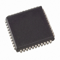
ATF1502ASV-15JU44 Atmel, ATF1502ASV-15JU44 Datasheet - Page 5

ATF1502ASV-15JU44
Manufacturer Part Number
ATF1502ASV-15JU44
Description
IC CPLD EE HP 15NS 44-PLCC
Manufacturer
Atmel
Series
ATF1502ASVr
Datasheet
1.ATF1502ASV-15AU44.pdf
(25 pages)
Specifications of ATF1502ASV-15JU44
Programmable Type
In System Programmable (min 10K program/erase cycles)
Delay Time Tpd(1) Max
15.0ns
Voltage Supply - Internal
3 V ~ 3.6 V
Number Of Macrocells
32
Number Of I /o
32
Operating Temperature
-40°C ~ 85°C
Mounting Type
Surface Mount
Package / Case
44-PLCC
Voltage
3.0 V ~ 3.6 V
Memory Type
EEPROM
Family Name
ATF1502ASV
# Macrocells
32
Number Of Usable Gates
750
Frequency (max)
100MHz
Propagation Delay Time
15ns
Number Of Logic Blocks/elements
2
# I/os (max)
32
Operating Supply Voltage (typ)
3.3V
In System Programmable
Yes
Operating Supply Voltage (min)
3V
Operating Supply Voltage (max)
3.6V
Operating Temp Range
-40C to 85C
Operating Temperature Classification
Industrial
Mounting
Surface Mount
Pin Count
44
Package Type
PLCC
Number Of Product Terms Per Macro
40
Maximum Operating Frequency
100 MHz
Delay Time
15 ns
Number Of Programmable I/os
32
Operating Supply Voltage
3.3 V
Maximum Operating Temperature
+ 85 C
Minimum Operating Temperature
- 40 C
Mounting Style
SMD/SMT
Supply Voltage (max)
3.6 V
Supply Voltage (min)
3 V
For Use With
ATF15XX-DK3 - KIT DEV FOR ATF15XX CPLD'S
Lead Free Status / RoHS Status
Lead free / RoHS Compliant
Features
-
Number Of Logic Elements/cells
-
Lead Free Status / Rohs Status
Compliant
Available stocks
Company
Part Number
Manufacturer
Quantity
Price
Part Number:
ATF1502ASV-15JU44
Manufacturer:
ATMEL/爱特梅尔
Quantity:
20 000
1.3
1.4
1.5
1.6
1.7
2. Programmable Pin-keeper Option for Inputs and I/Os
1615J–PLD–01/06
Flip-flop
Extra Feedback
I/O Control
Global Bus/Switch Matrix
Foldback Bus
The ATF1502ASV’s flip-flop has very flexible data and control functions. The data input can
come from either the XOR gate, from a separate product term or directly from the I/O pin. Select-
ing the separate product term allows creation of a buried registered feedback within a
combinatorial output macrocell. (This feature is automatically implemented by the fitter soft-
ware). In addition to D, T, JK and SR operation, the flip-flop can also be configured as a flow-
through latch. In this mode, data passes through when the clock is high and is latched when the
clock is low.
The clock itself can be either one of the Global CLK signals (GCK[0 : 2]) or an individual product
term. The flip-flop changes state on the clock’s rising edge. When the GCK signal is used as the
clock, one of the macrocell product terms can be selected as a clock enable. When the clock
enable function is active and the enable signal (product term) is low, all clock edges are ignored.
The flip-flop’s asynchronous reset signal (AR) can be either the Global Clear (GCLEAR), a prod-
uct term, or always off. AR can also be a logic OR of GCLEAR with a product term. The
asynchronous preset (AP) can be a product term or always off.
The ATF1502ASV macrocell output can be selected as registered or combinatorial.The extra
buried feedback signal can be either combinatorial or a registered signal regardless of whether
the output is combinatorial or registered. (This enhancement function is automatically imple-
mented by the fitter software.) Feedback of a buried combinatorial output allows the creation of a
second latch within a macrocell.
The output enable multiplexer (MOE) controls the output enable signal. Each I/O can be individ-
ually configured as an input, output or for bi-directional operation. The output enable for each
macrocell can be selected from the true or compliment of the two output enable pins, a subset of
the I/O pins, or a subset of the I/O macrocells. This selection is automatically done by the fitter
software when the I/O is configured as an input, all macrocell resources are still available,
including the buried feedback, expander and cascade logic.
The global bus contains all input and I/O pin signals as well as the buried feedback signal from
all 32 macrocells. The switch matrix in each logic block receives as its inputs all signals from the
global bus. Under software control, up to 40 of these signals can be selected as inputs to the
logic block.
Each macrocell also generates a foldback product term. This signal goes to the regional bus and
is available to four macrocells. The foldback is an inverse polarity of one of the macrocell’s prod-
uct terms. The four foldback terms in each region allow generation of high fan-in sum terms (up
to nine product terms) with little additional delay.
The ATF1502ASV offers the option of programming all input and I/O pins so that pin-keeper cir-
cuits can be utilized. When any pin is driven high or low and then subsequently left floating, it will
stay at that previous high or low level. This circuitry prevents unused input and I/O lines from
ATF1502ASV
5


