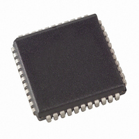
ATF2500C-20JC Atmel, ATF2500C-20JC Datasheet - Page 2

ATF2500C-20JC
Manufacturer Part Number
ATF2500C-20JC
Description
IC CPLD EE 20NS 44PLCC
Manufacturer
Atmel
Series
ATF2500C(L)r
Datasheet
1.ATF2500C-20JC.pdf
(24 pages)
Specifications of ATF2500C-20JC
Programmable Type
In System Programmable
Delay Time Tpd(1) Max
20.0ns
Voltage Supply - Internal
4.75 V ~ 5.25 V
Number Of Macrocells
24
Number Of I /o
24
Operating Temperature
0°C ~ 70°C
Mounting Type
Surface Mount
Package / Case
44-PLCC
Voltage
5V
Memory Type
EEPROM
Package
44PLCC
Family Name
ATF2500C
Device System Gates
2500
Maximum Propagation Delay Time
20 ns
Number Of User I/os
24
Typical Operating Supply Voltage
5 V
Maximum Operating Frequency
50 MHz
Number Of Product Terms Per Macro
12
Delay Time
20 ns
Number Of Programmable I/os
23
Operating Supply Voltage
5 V
Supply Current
80 mA
Maximum Operating Temperature
+ 70 C
Minimum Operating Temperature
0 C
Mounting Style
SMD/SMT
Supply Voltage (max)
5.25 V
Supply Voltage (min)
4.75 V
Lead Free Status / RoHS Status
Contains lead / RoHS non-compliant
Features
-
Number Of Logic Elements/cells
-
Lead Free Status / Rohs Status
Lead free / RoHS Compliant
Available stocks
Company
Part Number
Manufacturer
Quantity
Price
Company:
Part Number:
ATF2500C-20JC
Manufacturer:
ST
Quantity:
1 109
Part Number:
ATF2500C-20JC
Manufacturer:
ATMEL/爱特梅尔
Quantity:
20 000
2. Pin Configurations
2
ATF2500C
The ATF2500C is organized around a single universal array. All pins and feedback terms are
always available to every macrocell. Each of the 38 logic pins are array inputs, as are the out-
puts of each flip-flop.
In the ATF2500C, four product terms are input to each sum term. Furthermore, each macrocell’s
three sum terms can be combined to provide up to 12 product terms per sum term with no per-
formance penalty. Each flip-flop is individually selectable to be either D- or T-type, providing
further logic compaction. Also, 24 of the flip-flops may be bypassed to provide internal combina-
torial feedback to the logic array.
Product terms provide individual clocks and asynchronous resets for each flip-flop. The flip-flops
may also be individually configured to have direct input pin clocking. Each output has its own
enable product term. Eight synchronous preset product terms serve local groups of either four or
eight flip-flops. Register preload functions are provided to simplify testing. All registers automati-
cally reset upon power-up.
Table 2-1.
Pin Name
IN
CLK/IN
I/O
I/O 0,2,4...
I/O 1,3,5...
GND
VCC
Figure 2-1.
CLK/IN
I/O17
I/O16
I/O15
I/O14
I/O13
I/O12
VCC
I/O0
I/O1
I/O2
I/O3
I/O4
I/O5
IN
IN
IN
IN
IN
IN
1
2
3
4
5
6
7
8
9
10
11
12
13
14
15
16
17
18
19
20
Pin Configurations
DIP
40
39
38
37
36
35
34
33
32
31
30
29
28
27
26
25
24
23
22
21
IN
IN
IN
IN
I/O6
I/O7
I/O8
I/O9
I/O10
I/O11
GND
I/O23
I/O22
I/O21
I/O20
I/O19
I/O18
IN
IN
IN
Function
Logic Inputs
Pin Clock and Input
Bi-directional Buffers
Even I/O Buffers
Odd I/O Buffers
Ground
+5V Supply
Figure 2-2.
Note:
(PLCC package) pin 4 and pin 26 GND connections are
not required, but are recommended for improved noise
immunity.
I/O17
I/O16
I/O15
I/O14
I/O13
VCC
VCC
I/O2
I/O3
I/O4
I/O5
PLCC
7
8
9
10
11
12
13
14
15
16
17
39
38
37
36
35
34
33
32
31
30
29
I/O7
I/O8
I/O9
I/O10
I/O11
GND
GND
I/O23
I/O22
I/O21
I/O20
0777K–PLD–1/24/08


