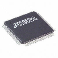
EPM3128ATC100-10N Altera, EPM3128ATC100-10N Datasheet - Page 11

EPM3128ATC100-10N
Manufacturer Part Number
EPM3128ATC100-10N
Description
IC MAX 3000A CPLD 128 100-TQFP
Manufacturer
Altera
Series
MAX® 3000Ar
Datasheet
1.EPM3032ATC44-10N.pdf
(46 pages)
Specifications of EPM3128ATC100-10N
Programmable Type
In System Programmable
Delay Time Tpd(1) Max
10.0ns
Voltage Supply - Internal
3 V ~ 3.6 V
Number Of Logic Elements/blocks
8
Number Of Macrocells
128
Number Of Gates
2500
Number Of I /o
80
Operating Temperature
0°C ~ 85°C
Mounting Type
Surface Mount
Package / Case
100-TQFP, 100-VQFP
Voltage
3.3V
Memory Type
EEPROM
Number Of Logic Elements/cells
8
Lead Free Status / RoHS Status
Lead free / RoHS Compliant
Features
-
Other names
544-1981
EPM3128ATC100-10N
EPM3128ATC100-10N
Available stocks
Company
Part Number
Manufacturer
Quantity
Price
Company:
Part Number:
EPM3128ATC100-10N
Manufacturer:
ST
Quantity:
12 560
Company:
Part Number:
EPM3128ATC100-10N
Manufacturer:
ALTERA
Quantity:
1 260
Company:
Part Number:
EPM3128ATC100-10N
Manufacturer:
ALTERA
Quantity:
178
Company:
Part Number:
EPM3128ATC100-10N
Manufacturer:
ALTERA108
Quantity:
4 827
Part Number:
EPM3128ATC100-10N
Manufacturer:
ALTERA/阿尔特拉
Quantity:
20 000
MAX 3000A Programmable Logic Device Family Data Sheet
Figure 5. MAX 3000A PIA Routing
To LAB
PIA Signals
While the routing delays of channel–based routing schemes in masked or
FPGAs are cumulative, variable, and path–dependent, the MAX 3000A
PIA has a predictable delay. The PIA makes a design’s timing
performance easy to predict.
I/O Control Blocks
The I/O control block allows each I/O pin to be individually configured
for input, output, or bidirectional operation. All I/O pins have a tri–state
buffer that is individually controlled by one of the global output enable
signals or directly connected to ground or V
.
Figure 6
shows the I/O
CC
control block for MAX 3000A devices. The I/O control block has 6 or
10 global output enable signals that are driven by the true or complement
of two output enable signals, a subset of the I/O pins, or a subset of the
I/O macrocells.
Altera Corporation
11


