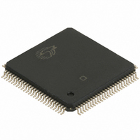
CY37128P100-125AXC Cypress Semiconductor Corp, CY37128P100-125AXC Datasheet - Page 4

CY37128P100-125AXC
Manufacturer Part Number
CY37128P100-125AXC
Description
IC CPLD 128 MACROCELL 100-LQFP
Manufacturer
Cypress Semiconductor Corp
Series
Ultra37000™r
Specifications of CY37128P100-125AXC
Number Of Macrocells
128
Package / Case
100-LQFP
Programmable Type
In-System Reprogrammable™ (ISR™) CMOS
Delay Time Tpd(1) Max
10.0ns
Voltage Supply - Internal
4.75 V ~ 5.25 V
Number Of I /o
69
Operating Temperature
0°C ~ 70°C
Mounting Type
Surface Mount
Features
Programmable
Voltage
5V
Memory Type
CMOS
Number Of Product Terms Per Macro
16
Maximum Operating Frequency
125 MHz
Delay Time
10 ns
Number Of Programmable I/os
69
Operating Supply Voltage
5 V
Maximum Operating Temperature
+ 70 C
Minimum Operating Temperature
0 C
Mounting Style
SMD/SMT
Supply Voltage (max)
5.25 V
Supply Voltage (min)
4.75 V
Family Name
Ultra 37000
# Macrocells
128
Number Of Usable Gates
3800
Frequency (max)
125MHz
Propagation Delay Time
10ns
Number Of Logic Blocks/elements
8
# I/os (max)
69
Operating Supply Voltage (typ)
5V
In System Programmable
Yes
Operating Supply Voltage (min)
4.75V
Operating Supply Voltage (max)
5.25V
Operating Temp Range
0C to 70C
Operating Temperature Classification
Commercial
Mounting
Surface Mount
Pin Count
100
Package Type
TQFP
Lead Free Status / RoHS Status
Lead free / RoHS Compliant
For Use With
CY3710 - ADAPTER SOCKET PTG
Number Of Logic Elements/cells
-
Lead Free Status / Rohs Status
Lead free / RoHS Compliant
Other names
428-2903
CY37128P100-125AXC
CY37128P100-125AXC
Available stocks
Company
Part Number
Manufacturer
Quantity
Price
Company:
Part Number:
CY37128P100-125AXC
Manufacturer:
CYPRESS
Quantity:
225
Company:
Part Number:
CY37128P100-125AXC
Manufacturer:
Cypress Semiconductor Corp
Quantity:
10 000
Architecture Overview of Ultra37000 Family
Programmable Interconnect Matrix
The PIM consists of a completely global routing matrix for signals
from I/O pins and feedbacks from the logic blocks. The PIM
provides extremely robust interconnection to avoid fitting and
density limitations.
The inputs to the PIM consist of all I/O and dedicated input pins
and all macrocell feedbacks from within the logic blocks. The
number of PIM inputs increases with pin count and the number
of logic blocks. The outputs from the PIM are signals routed to
the appropriate logic blocks. Each logic block receives 36 inputs
from the PIM and their complements, allowing for 32-bit opera-
tions to be implemented in a single pass through the device. The
wide number of inputs to the logic block also improves the routing
capacity of the Ultra37000 family.
An important feature of the PIM is its simple timing. The propa-
gation delay through the PIM is accounted for in the timing speci-
fications for each device. There is no additional delay for
traveling through the PIM. In fact, all inputs travel through the
PIM. As a result, there are no route-dependent timing param-
eters on the Ultra37000 devices. The worst-case PIM delays are
incorporated in all appropriate Ultra37000 specifications.
Routing signals through the PIM is completely invisible to the
user. All routing is accomplished by software—no hand routing
is necessary. Warp
automatically route designs for the Ultra37000 family in a matter
of minutes. Finally, the rich routing resources of the Ultra37000
family accommodate last minute logic changes while maintaining
fixed pin assignments.
Document Number : 38-03007 Rev. *H
FROM
PIM
TO
PIM
36
and third-party development packages
PRODUCT TERM
72 x 87
ARRAY
Figure 1. Logic Block with 50% Buried Macrocells
80
7
16
8
ALLOCATOR
PRODUCT
TERM
Logic Block
The logic block is the basic building block of the Ultra37000
architecture. It consists of a product term array, an intelligent
product-term allocator, 16 macrocells, and a number of I/O cells.
The number of I/O cells varies depending on the device used.
Refer to
Product Term Array
Each logic block features a 72 x 87 programmable product term
array. This array accepts 36 inputs from the PIM, which originate
from macrocell feedbacks and device pins. Active LOW and
active HIGH versions of each of these inputs are generated to
create the full 72-input field. The 87 product terms in the array
can be created from any of the 72 inputs.
Of the 87 product terms, 80 are for general-purpose use for the
16 macrocells in the logic block. Four of the remaining seven
product terms in the logic block are output enable (OE) product
terms. Each of the OE product terms controls up to eight of the
16 macrocells and is selectable on an individual macrocell basis.
In other words, each I/O cell can select between one of two OE
product terms to control the output buffer. The first two of these
four OE product terms are available to the upper half of the I/O
macrocells in a logic block. The other two OE product terms are
available to the lower half of the I/O macrocells in a logic block.
The next two product terms in each logic block are dedicated
asynchronous set and asynchronous reset product terms. The
final product term is the product term clock. The set, reset, OE
and product term clock have polarity control to realize OR
functions in a single pass through the array.
PRODUCT
PRODUCT
PRODUCT
PRODUCT
TERMS
TERMS
TERMS
TERMS
016
016
016
016
Figure 1
MACRO-
MACRO-
MACRO-
MACRO-
CELL
CELL
CELL
CELL
14
15
for the block diagram.
0
1
3
Ultra37000 CPLD Family
CELL
CELL
I/O
I/O
14
0
to cells
2, 4, 6 8, 10, 12
2
2
Page 4 of 43
[+] Feedback


