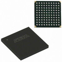
EPM240F100C5N Altera, EPM240F100C5N Datasheet - Page 63

EPM240F100C5N
Manufacturer Part Number
EPM240F100C5N
Description
IC MAX II CPLD 240 LE 100-FBGA
Manufacturer
Altera
Series
MAX® IIr
Specifications of EPM240F100C5N
Programmable Type
In System Programmable
Delay Time Tpd(1) Max
4.7ns
Voltage Supply - Internal
2.5V, 3.3V
Number Of Logic Elements/blocks
240
Number Of Macrocells
192
Number Of I /o
80
Operating Temperature
0°C ~ 85°C
Mounting Type
Surface Mount
Package / Case
100-FBGA
Voltage
2.5V, 3.3V
Memory Type
FLASH
Number Of Logic Elements/cells
240
Family Name
MAX II
# Macrocells
192
Frequency (max)
1.8797GHz
Propagation Delay Time
7.5ns
Number Of Logic Blocks/elements
24
# I/os (max)
80
Operating Supply Voltage (typ)
2.5/3.3V
In System Programmable
Yes
Operating Supply Voltage (min)
2.375V
Operating Supply Voltage (max)
3.6V
Operating Temp Range
0C to 85C
Operating Temperature Classification
Commercial
Mounting
Surface Mount
Pin Count
100
Package Type
FBGA
Lead Free Status / RoHS Status
Lead free / RoHS Compliant
Features
-
Lead Free Status / Rohs Status
Compliant
Other names
544-1709
Available stocks
Company
Part Number
Manufacturer
Quantity
Price
Company:
Part Number:
EPM240F100C5N
Manufacturer:
NSC
Quantity:
560
Company:
Part Number:
EPM240F100C5N
Manufacturer:
ALTERA
Quantity:
591
Part Number:
EPM240F100C5N
Manufacturer:
ALTERA/阿尔特拉
Quantity:
20 000
Chapter 5: DC and Switching Characteristics
Operating Conditions
Output Drive Characteristics
Figure 5–1. Output Drive Characteristics of MAX II Devices
Note to
(1) The DC output current per pin is subject to the absolute maximum rating of
I/O Standard Specifications
Table 5–5. 3.3-V LVTTL Specifications
Table 5–6. 3.3-V LVCMOS Specifications (Part 1 of 2)
© August 2009 Altera Corporation
V
V
V
V
V
V
V
V
CCIO
IH
IL
OH
OL
CCIO
IH
IL
Symbol
Symbol
Figure
5–1:
I/O supply voltage
High-level input voltage
Low-level input voltage
High-level output voltage
Low-level output voltage
I/O supply voltage
High-level input voltage
Low-level input voltage
70
60
50
40
30
20
10
35
30
25
20
15
10
0
5
0
0.0
0.0
3.3-V VCCIO
2.5-V VCCIO
1.8-V VCCIO
1.5-V VCCIO
MAX II Output Drive I
Parameter
Parameter
0.5
Figure 5–1
3.3-V VCCIO
2.5-V VCCIO
1.8-V VCCIO
1.5-V VCCIO
Table 5–5
specifications.
0.5
MAX II Output Drive I
(Maximum Drive Strength)
1.0
(Minimum Drive Strength)
1.0
1.5
Voltage (V)
1.5
Voltage (V)
through
OH
shows the typical drive strength characteristics of MAX II devices.
OH
Characteristics
2.0
Characteristics
2.0
IOH = –4 mA
IOL = 4 mA
2.5
2.5
Table 5–10
Conditions
Conditions
3.0
3.0
—
—
—
—
—
—
3.5
3.5
(1)
(1)
show the MAX II device family I/O standard
Minimum
Minimum
Table
–0.5
30
25
20
15
10
3.0
1.7
2.4
60
50
40
30
20
10
—
5
0
0
0.0
–0.5
0.0
3.0
1.7
5–1.
0.5
0.5
MAX II Output Drive I
MAX II Output Drive I
1.5-V VCCIO
1.0
(Minimum Drive Strength)
1.0
1.5-V VCCIO
(Maximum Drive Strength)
Maximum
1.8-V VCCIO
1.8-V VCCIO
Maximum
1.5
1.5
Voltage (V)
Voltage (V)
0.45
3.6
4.0
0.8
—
3.6
4.0
0.8
OL
OL
Characteristics
2.5-V VCCIO
2.0
2.0
2.5-V VCCIO
Characteristics
2.5
2.5
3.3-V VCCIO
3.3-V VCCIO
Unit
Unit
3.0
3.0
V
V
V
V
V
V
V
V
MAX II Device Handbook
3.5
3.5
5–5


