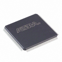
EPM1270T144C4 Altera, EPM1270T144C4 Datasheet - Page 35

EPM1270T144C4
Manufacturer Part Number
EPM1270T144C4
Description
IC MAX II CPLD 1270 LE 144-TQFP
Manufacturer
Altera
Series
MAX® IIr
Specifications of EPM1270T144C4
Programmable Type
In System Programmable
Delay Time Tpd(1) Max
6.2ns
Voltage Supply - Internal
2.5V, 3.3V
Number Of Logic Elements/blocks
1270
Number Of Macrocells
980
Number Of I /o
116
Operating Temperature
0°C ~ 85°C
Mounting Type
Surface Mount
Package / Case
144-TQFP, 144-VQFP
Voltage
2.5V, 3.3V
Memory Type
FLASH
Number Of Logic Elements/cells
1270
For Use With
544-2380 - KIT DEV MAXII W/EPM 1270N
Lead Free Status / RoHS Status
Contains lead / RoHS non-compliant
Features
-
Other names
544-1142
544-1325
544-1325
EPM1270T144C4ES
544-1325
544-1325
EPM1270T144C4ES
Available stocks
Company
Part Number
Manufacturer
Quantity
Price
Part Number:
EPM1270T144C4N
Manufacturer:
ALTERA/阿尔特拉
Quantity:
20 000
Chapter 2: MAX II Architecture
I/O Structure
Figure 2–22. MAX II I/O Banks for EPM240 and EPM570
Notes to
(1)
(2)
© October 2008 Altera Corporation
Figure 2–22
Figure 2–22
Figure
2–22:
is a top view of the silicon die.
is a graphical representation only. Refer to the pin list and the Quartus II software for exact pin locations.
I/O Bank 1
Table 2–4
Table 2–4. MAX II I/O Standards
The EPM240 and EPM570 devices support two I/O banks, as shown in
Each of these banks support all the LVTTL and LVCMOS standards shown in
Table
The EPM1270 and EPM2210 devices support four I/O banks, as shown in
Each of these banks support all of the LVTTL and LVCMOS standards shown in
Table
clamping diode on inputs and PCI drive compliance on outputs. You must use Bank 3
for designs requiring PCI compliant I/O pins. The Quartus II software automatically
places I/O pins in this bank if assigned with the PCI I/O standard.
3.3-V LVTTL/LVCMOS
2.5-V LVTTL/LVCMOS
1.8-V LVTTL/LVCMOS
1.5-V LVCMOS
3.3-V PCI
Note to
(1) The 3.3-V PCI compliant I/O is supported in Bank 3 of the EPM1270 and EPM2210
devices.
I/O Standard
2–4. PCI compliant I/O is not supported in these devices and banks.
2–4. PCI compliant I/O is supported in Bank 3. Bank 3 supports the PCI
Table
(1)
describes the I/O standards supported by MAX II devices.
2–4:
All I/O Banks Support
■
■
■
■
3.3-V LVTTL/LVCMOS
2.5-V LVTTL/LVCMOS
1.8-V LVTTL/LVCMOS
1.5-V LVCMOS
Single-ended
Single-ended
Single-ended
Single-ended
Single-ended
(Note
Type
1),
(2)
Output Supply Voltage
(VCCIO) (V)
3.3
2.5
1.8
1.5
3.3
I/O Bank 2
MAX II Device Handbook
Figure
Figure
2–22.
2–23.
2–27


