SS103VD10CAQLF7 BI Technologies, SS103VD10CAQLF7 Datasheet

Resistor Networks & Arrays 10K ohm 10K ohm

SS103VD10CAQLF7

Manufacturer Part Number
SS103VD10CAQLF7
Description
Resistor Networks & Arrays 10K ohm 10K ohm
Manufacturer
BI Technologies
Series
SS103VDr
Datasheet

Specifications of SS103VD10CAQLF7

Product Type
Networks
Circuit Type
Divider
Number Of Resistors
2
Resistance
10 KOhms, 10 KOhms
Tolerance
25 %
Power Rating
0.2 Watt (1/5 Watt)
Temperature Coefficient
+/- 25 PPM / C
Number Of Pins
3
Package / Case
SOT-23
Operating Temperature Range
- 55 C to + 125 C
Termination Style
SMD/SMT
Voltage Rating
100 Volts
Lead Free Status / Rohs Status
Lead free / RoHS Compliant
MODELS
SS103VD, SFN06VD
Voltage divider circuit
Thin film resistor network
RoHS compliant available
FEATURES
Precision Nichrome Resistors on Silicon
Industry Standard Packaging
Ratio Tolerances
TCR Tracking Tolerances
CIRCUIT SCHEMATIC
ELECTRICAL
Standard Resistance Range
Resistor Tolerances
Ratio Tolerances
TCR
Operating Temperature Range
Interlead Capacitance
Insulation Resistance
Maximum Operating Voltage
Noise, Maximum (MIL-STD-2002, Method 308)
Maximum Package Power @ 70 C
RESISTANCE TOLERANCES
Accuracy Code at 25°C
Absolute Resistance Tolerances (%)
Ratio Tolerances (R1 Ref) (%)
1
2
BI Technologies Corporation
4200 Bonita Place
Fullerton, CA 92835 USA
Website:
May 6, 2009
Small outline no lead (SON) package is also referred to as quad flat no lead (QFN) or dual flat no lead (DFN) packages.
Specifications subject to change without notice.
www.bitechnologies.com
2
± 0.25
± 0.05
CA
page 1 of 3
± 0.25
± 0.1
CB
6 pad SON
Passivation coating provides protection in humid environments
± 0.5
± 0.1
D
1
2mm square with 0.65 mm pitch (JEDEC MO-229D)
± 0.05
± 1.0
FA
3 lead SOT23 (JEDEC TO-239)
± 1.0
± 1.0
F
BI technologies
1K ohms to 100K ohms
Reference TCR table
= 10,000 Megohms
± 2.0
N/A
G
-55 C to +125 C
100 Vdc or v PR
< ± 5 ppm/°C
< ± 0.05%
0.2 Watts
± 0.25%
± 0.05%
± 5.0
-25 dB
N/A
< 2 pF
J

Related parts for SS103VD10CAQLF7

SS103VD10CAQLF7 Summary of contents

Page 1

... Absolute Resistance Tolerances (%) Ratio Tolerances (R1 Ref) (%) 1 Small outline no lead (SON) package is also referred to as quad flat no lead (QFN) or dual flat no lead (DFN) packages. 2 Specifications subject to change without notice. BI Technologies Corporation 4200 Bonita Place Fullerton, CA 92835 USA Website: www.bitechnologies.com May 6, 2009 Passivation coating provides protection in humid environments ...

Page 2

... Marking Permanency Storage Temperature Range MECHANICAL Lead Plating Lead Material Lead Configurations (SLP/SS1) Lead Coplanarity (SS1 only) Substrate Material Resistor Material Body Material Package Types BI Technologies Corporation 4200 Bonita Place Fullerton, CA 92835 USA Website: www.bitechnologies.com May 6, 2009 Q P ± 25 ± 50 ± 5 ± ...

Page 3

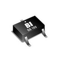
... S1 = SOT- SON 2mm sq Pin Count: Circuit Type: VD=Voltage Divider Resistance Code: Divider ratio table TYPICAL MARKING 3 Contact our customer service for custom designs and features. BI Technologies Corporation 4200 Bonita Place Fullerton, CA 92835 USA Website: www.bitechnologies.com May 6, 2009 R1 (ohms) 1.613 12.4K 10 10K ...

Related keywords