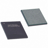
EP1C12F324C6 Altera, EP1C12F324C6 Datasheet - Page 74

EP1C12F324C6
Manufacturer Part Number
EP1C12F324C6
Description
IC CYCLONE FPGA 12K LE 324-FBGA
Manufacturer
Altera
Series
Cyclone®r
Datasheet
1.EP1C3T144C8.pdf
(106 pages)
Specifications of EP1C12F324C6
Number Of Logic Elements/cells
12060
Number Of Labs/clbs
1206
Total Ram Bits
239616
Number Of I /o
249
Voltage - Supply
1.425 V ~ 1.575 V
Mounting Type
Surface Mount
Operating Temperature
0°C ~ 85°C
Package / Case
324-FBGA
Family Name
Cyclone®
Number Of Logic Blocks/elements
12060
# I/os (max)
249
Frequency (max)
405.2MHz
Process Technology
0.13um (CMOS)
Operating Supply Voltage (typ)
1.5V
Logic Cells
12060
Ram Bits
239616
Operating Supply Voltage (min)
1.425V
Operating Supply Voltage (max)
1.575V
Operating Temp Range
0C to 85C
Operating Temperature Classification
Commercial
Mounting
Surface Mount
Pin Count
324
Package Type
FBGA
Lead Free Status / RoHS Status
Contains lead / RoHS non-compliant
Number Of Gates
-
Lead Free Status / Rohs Status
Not Compliant
Other names
544-1034
Available stocks
Company
Part Number
Manufacturer
Quantity
Price
Company:
Part Number:
EP1C12F324C6
Manufacturer:
ALTERA
Quantity:
7
Company:
Part Number:
EP1C12F324C6
Manufacturer:
ALTERA
Quantity:
1 831
Company:
Part Number:
EP1C12F324C6
Manufacturer:
ALTERA
Quantity:
210
Company:
Part Number:
EP1C12F324C6AA
Manufacturer:
ALTERA
Quantity:
3 000
Company:
Part Number:
EP1C12F324C6N
Manufacturer:
ALTERA
Quantity:
5
Cyclone Device Handbook, Volume 1
4–4
Preliminary
V
V
V
V
V
V
V
Δ V
V
Δ V
V
V
R
V
V
V
Table 4–8. 1.5-V I/O Specifications
Table 4–9. 2.5-V LVDS I/O Specifications
Table 4–10. 3.3-V PCI Specifications (Part 1 of 2)
CCIO
I H
IL
OH
OL
CCIO
OD
OS
TH
IN
CCIO
IH
IL
L
Symbol
Symbol
Symbol
OD
OS
Output supply voltage
High-level input voltage
Low-level input voltage
High-level output voltage
Low-level output voltage
I/O supply voltage
Differential output voltage
Change in V
high and low
Output offset voltage
Change in V
high and low
Differential input threshold V
Receiver input voltage
range
Receiver differential input
resistor
Output supply voltage
High-level input voltage
Low-level input voltage
Parameter
Parameter
Parameter
OD
OS
between
between
R
R
R
R
CM
L
L
L
L
= 100 Ω
= 100 Ω
= 100 Ω
= 100 Ω
= 1.2 V
Note (13)
Conditions
Conditions
I
I
OH
OL
—
—
—
—
—
—
= 2 mA
= –2 mA
Conditions
—
—
—
(11)
(11)
Minimum
Minimum
2.375
1.125
0.5 ×
V
–100
–0.5
250
0.0
3.0
90
—
—
CCIO
Minimum
0.65 ×
0.75 ×
V
V
–0.3
1.4
CCIO
CCIO
—
Typical
Typical
1.25
100
2.5
3.3
—
—
—
—
—
—
—
V
Maximum
CCIO
Maximum
Maximum
0.35 ×
0.25 ×
Altera Corporation
V
V
V
(12)
2.625
1.375
0.3 ×
V
1.6
CCIO
CCIO
CCIO
—
550
100
110
2.4
3.6
0.5
50
50
CCIO
+ 0.3
+
May 2008
Unit
Unit
Unit
mV
mV
mV
mV
V
V
V
V
V
V
V
V
Ω
V
V
V


