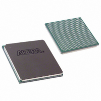
EP3C40F780C7N Altera, EP3C40F780C7N Datasheet - Page 31

EP3C40F780C7N
Manufacturer Part Number
EP3C40F780C7N
Description
IC CYCLONE III FPGA 40K 780FBGA
Manufacturer
Altera
Series
Cyclone® IIIr
Datasheets
1.EP3C5F256C8N.pdf
(5 pages)
2.EP3C5F256C8N.pdf
(34 pages)
3.EP3C5F256C8N.pdf
(66 pages)
4.EP3C5F256C8N.pdf
(14 pages)
5.EP3C5F256C8N.pdf
(76 pages)
Specifications of EP3C40F780C7N
Number Of Logic Elements/cells
39600
Number Of Labs/clbs
2475
Total Ram Bits
1161216
Number Of I /o
535
Voltage - Supply
1.15 V ~ 1.25 V
Mounting Type
Surface Mount
Operating Temperature
0°C ~ 85°C
Package / Case
780-FBGA
For Use With
544-2601 - KIT DEV CYCLONE III LS EP3CLS200544-2411 - KIT DEV NIOS II CYCLONE III ED.
Lead Free Status / RoHS Status
Lead free / RoHS Compliant
Number Of Gates
-
Other names
544-2503
Available stocks
Company
Part Number
Manufacturer
Quantity
Price
Design and Compilation
© November 2008 Altera Corporation
f
Figure 3. Synchronous Design
If the combinational logic output from your design feeds to another part of the design,
have the signal go through a register, as illustrated in
using the combinational logic output as a clock signal or as an asynchronous reset
signal. Due to propagation delays through the combinational logic, the signal may go
through a number of transitions before the output settles to a new value. This means
changes to the combinational output can trigger a period of instability.
As the input of the register is only sampled and transferred to the design (for
example, the combinational logic 2 shown in
clock, transitions taking place on data inputs of the register do not affect the register
output or input to the other part of the design until the next active clock edge. As long
as the setup and hold time of the register is not violated, the register effectively
isolates any glitches or instable input signals from other logics.
Figure 4. Registering Combinational Output Signal
It is recommended that you register the input signals to the device as well to filter out
any glitches. The Cyclone III I/Os have input registers for this purpose. Using the
input registers for your input signals allows faster setup times compared to using the
LE registers. This can be done with the Fast Input Register assignment.
Also, your design should not rely on delay paths within the architecture of a device,
for example using the LCELL primitives to increase the delay of certain signals in the
design because factors such as temperature, voltage, process change, or placement
and routing change could affect the timing of logic paths in the device. Any change in
timing to a specific path could cause unwanted functional changes and affect the
design functionality. Synchronization eliminates the unwanted functional changes.
For more information about synchronizing your design, refer to the
Recommendations for Altera Devices and the Quartus II Design Assistant
volume 1 of the Quartus II Handbook or the Quartus II Help.
Combinational
clock
Logic 1
clock
D
Q
D
Q
Figure
D
Combinational
4) on every active edge of the
Table
Logic 2
Q
4. This applies if you are
Design
chapter in
Page 31


