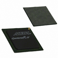
EP2C70F896I8N Altera, EP2C70F896I8N Datasheet - Page 85

EP2C70F896I8N
Manufacturer Part Number
EP2C70F896I8N
Description
IC CYCLONE II FPGA 70K 896-FBGA
Manufacturer
Altera
Series
Cyclone® IIr
Datasheet
1.EP2C5T144C8N.pdf
(168 pages)
Specifications of EP2C70F896I8N
Number Of Logic Elements/cells
68416
Number Of Labs/clbs
4276
Total Ram Bits
1152000
Number Of I /o
622
Voltage - Supply
1.15 V ~ 1.25 V
Mounting Type
Surface Mount
Operating Temperature
-40°C ~ 100°C
Package / Case
896-FBGA
Family Name
Cyclone® II
Number Of Logic Blocks/elements
68416
# I/os (max)
622
Frequency (max)
402.58MHz
Process Technology
90nm
Operating Supply Voltage (typ)
1.2V
Logic Cells
68416
Ram Bits
1152000
Operating Supply Voltage (min)
1.15V
Operating Supply Voltage (max)
1.25V
Operating Temp Range
-40C to 100C
Operating Temperature Classification
Industrial
Mounting
Surface Mount
Pin Count
896
Package Type
FBGA
For Use With
P0304 - DE2-70 CALL FOR ACADEMIC PRICING544-1703 - VIDEO KIT W/CYCLONE II EP2C70N544-1699 - DSP KIT W/CYCLONE II EPS2C70N
Lead Free Status / RoHS Status
Lead free / RoHS Compliant
Number Of Gates
-
Lead Free Status / Rohs Status
Compliant
Other names
544-2147
Available stocks
Company
Part Number
Manufacturer
Quantity
Price
Company:
Part Number:
EP2C70F896I8N
Manufacturer:
ALTERA21
Quantity:
196
Part Number:
EP2C70F896I8N
Manufacturer:
ALTERA/阿尔特拉
Quantity:
20 000
Hot-Socketing
Feature
Implementation
in Cyclone II
Devices
Altera Corporation
February 2007
the power supply can provide current to the device’s V
planes. This condition can lead to latch-up and cause a low-impedance
path from V
a large amount of current, possibly causing electrical damage.
Altera has ensured by design of the I/O buffers and hot-socketing
circuitry, that Cyclone II devices are immune to latch-up during hot
socketing.
The hot-socketing feature turns off the output buffer during power up
(either V
generates an internal HOTSCKT signal when either V
below the threshold voltage. Designs cannot use the HOTSCKT signal for
other purposes. The HOTSCKT signal cuts off the output buffer to ensure
that no DC current (except for weak pull-up leakage current) leaks
through the pin. When V
even after the internal POR signal (not available to the FPGA fabric used
by customer designs) is released and the configuration is finished. The
CONF_DONE, nCEO, and nSTATUS pins fail to respond, as the output
buffer cannot drive out because the hot-socketing circuitry keeps the I/O
pins tristated at this low V
has been removed on these configuration output or bidirectional pins to
ensure that they are able to operate during configuration. These pins are
expected to drive out during power-up and power-down sequences.
Each I/O pin has the circuitry shown in
CCINT
CC
or V
to ground within the device. As a result, the device extends
CCIO
supplies) or power down. The hot-socket circuit
CC
CC
ramps up slowly, V
voltage. Therefore, the hot-socketing circuit
Cyclone II Device Handbook, Volume 1
Figure
Hot Socketing & Power-On Reset
CC
4–1.
is still relatively low
CCINT
CC
and ground
or V
CCIO
is
4–3


