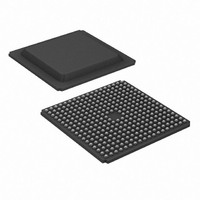
XC3S1600E-4FGG320C Xilinx Inc, XC3S1600E-4FGG320C Datasheet - Page 118

XC3S1600E-4FGG320C
Manufacturer Part Number
XC3S1600E-4FGG320C
Description
IC SPARTAN-3E FPGA 1600K 320-FBG
Manufacturer
Xilinx Inc
Series
Spartan™-3Er
Datasheet
1.XC3S100E-4VQG100C.pdf
(233 pages)
Specifications of XC3S1600E-4FGG320C
Number Of Logic Elements/cells
33192
Number Of Labs/clbs
3688
Total Ram Bits
663552
Number Of I /o
250
Number Of Gates
1600000
Voltage - Supply
1.14 V ~ 1.26 V
Mounting Type
Surface Mount
Operating Temperature
0°C ~ 85°C
Package / Case
320-BGA
For Use With
HW-XA3S1600E-UNI-G - KIT DEVELOPMENT AUTOMOTIVE ECU
Lead Free Status / RoHS Status
Lead free / RoHS Compliant
Other names
122-1481
Available stocks
Company
Part Number
Manufacturer
Quantity
Price
Company:
Part Number:
XC3S1600E-4FGG320C
Manufacturer:
XILINX
Quantity:
560
Company:
Part Number:
XC3S1600E-4FGG320C
Manufacturer:
XILINX
Quantity:
2 050
Company:
Part Number:
XC3S1600E-4FGG320C
Manufacturer:
XILINX
Quantity:
247
Part Number:
XC3S1600E-4FGG320C
Manufacturer:
XILINX/赛灵思
Quantity:
20 000
DC and Switching Characteristics
Power Supply Specifications
Table 74: Supply Voltage Thresholds for Power-On Reset
Table 75: Supply Voltage Ramp Rate
Table 76: Supply Voltage Levels Necessary for Preserving RAM Contents
118
Notes:
1.
2.
Notes:
1.
2.
Notes:
1.
V
SPI Flash, parallel NOR Flash, microcontroller) might have specific requirements. Check the data sheet for the attached configuration
source. In Step 0 devices using the HSWAP internal pull-up, V
To ensure successful power-on, V
no dips at any point.
V
SPI Flash, parallel NOR Flash, microcontroller) might have specific requirements. Check the data sheet for the attached configuration
source. In Step 0 devices using the HSWAP internal pull-up, V
To ensure successful power-on, V
no dips at any point.
Symbol
RAM contents include configuration data.
V
V
CCINT
CCINT
DRAUX
V
V
DRINT
V
Symbol
V
Symbol
V
V
CCAUXR
CCAUXT
CCINTR
CCINTT
CCO2R
CCO2T
, V
, V
CCAUX
CCAUX
, and V
, and V
V
V
CCINT
CCAUX
Threshold for the V
Threshold for the V
Threshold for the V
Ramp rate from GND to valid V
Ramp rate from GND to valid V
Ramp rate from GND to valid V
CCO
CCO
level required to retain RAM data
level required to retain RAM data
supplies to the FPGA can be applied in any order. However, the FPGA’s configuration source (Platform Flash,
supplies to the FPGA can be applied in any order. However, the FPGA’s configuration source (Platform Flash,
CCINT
CCINT
, V
, V
CCO
CCO
CCINT
CCAUX
CCO
Bank 2, and V
Bank 2, and V
Description
Description
Bank 2 supply
supply
supply
Description
www.xilinx.com
CCINT
CCAUX
CCO
CCAUX
CCAUX
CCINT
CCINT
Bank 2 supply level
supply level
supplies must rise through their respective threshold-voltage ranges with
supplies must rise through their respective threshold-voltage ranges with
supply level
must be applied before V
must be applied before V
CCAUX
CCAUX
Min
Min
0.4
0.8
0.4
0.2
0.2
0.2
.
.
DS312-3 (v3.8) August 26, 2009
Max
Max
1.0
2.0
1.0
50
50
50
Product Specification
Min
1.0
2.0
Units
Units
Units
ms
ms
ms
V
V
V
V
V
R


