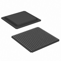
XC3S1600E-4FGG400C Xilinx Inc, XC3S1600E-4FGG400C Datasheet - Page 142

XC3S1600E-4FGG400C
Manufacturer Part Number
XC3S1600E-4FGG400C
Description
IC SPARTAN-3E FPGA 1600K 400FBGA
Manufacturer
Xilinx Inc
Series
Spartan™-3Er
Datasheet
1.XC3S100E-4VQG100C.pdf
(233 pages)
Specifications of XC3S1600E-4FGG400C
Number Of Logic Elements/cells
33192
Number Of Labs/clbs
3688
Total Ram Bits
663552
Number Of I /o
304
Number Of Gates
1600000
Voltage - Supply
1.14 V ~ 1.26 V
Mounting Type
Surface Mount
Operating Temperature
0°C ~ 85°C
Package / Case
400-BGA
For Use With
HW-XA3S1600E-UNI-G - KIT DEVELOPMENT AUTOMOTIVE ECU
Lead Free Status / RoHS Status
Lead free / RoHS Compliant
Other names
122-1517
Available stocks
Company
Part Number
Manufacturer
Quantity
Price
Company:
Part Number:
XC3S1600E-4FGG400C
Manufacturer:
XILINX
Quantity:
450
Company:
Part Number:
XC3S1600E-4FGG400C
Manufacturer:
XILINX
Quantity:
1 049
Company:
Part Number:
XC3S1600E-4FGG400C
Manufacturer:
Xilinx Inc
Quantity:
10 000
Part Number:
XC3S1600E-4FGG400C
Manufacturer:
XILINX/赛灵思
Quantity:
20 000
- Current page: 142 of 233
- Download datasheet (6Mb)
DC and Switching Characteristics
Block RAM Timing
Table 103: Block RAM Timing
142
Notes:
1.
Clock-to-Output Times
T
Setup Times
T
T
T
T
Hold Times
T
T
T
T
Clock Timing
T
T
Clock Frequency
F
Symbol
BCKO
BACK
BDCK
BECK
BWCK
BCKA
BCKD
BCKE
BCKW
BPWH
BPWL
BRAM
The numbers in this table are based on the operating conditions set forth in
When reading from block RAM, the delay from the
active transition at the CLK input to data appearing at
the DOUT output
Setup time for the ADDR inputs before the active
transition at the CLK input of the block RAM
Setup time for data at the DIN inputs before the active
transition at the CLK input of the block RAM
Setup time for the EN input before the active transition
at the CLK input of the block RAM
Setup time for the WE input before the active transition
at the CLK input of the block RAM
Hold time on the ADDR inputs after the active transition
at the CLK input
Hold time on the DIN inputs after the active transition at
the CLK input
Hold time on the EN input after the active transition at
the CLK input
Hold time on the WE input after the active transition at
the CLK input
High pulse width of the CLK signal
Low pulse width of the CLK signal
Block RAM clock frequency. RAM read output value
written back into RAM, for shift-registers and circular
buffers. Write-only or read-only performance is faster.
Description
www.xilinx.com
Table
0.33
0.23
0.67
1.09
0.12
0.12
1.39
1.39
Min
77.
0
0
0
-
-5
Max
2.45
270
Speed Grade
-
-
-
-
-
-
-
-
-
-
DS312-3 (v3.8) August 26, 2009
0.38
0.23
0.77
1.26
0.14
0.13
1.59
1.59
Min
0
0
0
-
-4
Product Specification
Max
2.82
230
-
-
-
-
-
-
-
-
-
-
Units
MHz
ns
ns
ns
ns
ns
ns
ns
ns
ns
ns
ns
R
Related parts for XC3S1600E-4FGG400C
Image
Part Number
Description
Manufacturer
Datasheet
Request
R

Part Number:
Description:
FPGA, SPARTAN-3E, 1600K GATES, 484FBGA
Manufacturer:
Xilinx Inc
Datasheet:

Part Number:
Description:
IC SPARTAN-3E FPGA 1600K 320-FBG
Manufacturer:
Xilinx Inc
Datasheet:

Part Number:
Description:
IC FPGA SPARTAN-3E 1600K 320FBGA
Manufacturer:
Xilinx Inc
Datasheet:

Part Number:
Description:
IC FPGA SPARTAN-3E 1600K 320FBGA
Manufacturer:
Xilinx Inc
Datasheet:

Part Number:
Description:
IC FPGA SPARTAN-3E 1600K 400FBGA
Manufacturer:
Xilinx Inc
Datasheet:

Part Number:
Description:
IC FPGA SPARTAN-3E 1600K 484FBGA
Manufacturer:
Xilinx Inc
Datasheet:

Part Number:
Description:
IC FPGA SPARTAN 3E 320FBGA
Manufacturer:
Xilinx Inc
Datasheet:

Part Number:
Description:
IC FPGA SPARTAN 3E 400FBGA
Manufacturer:
Xilinx Inc
Datasheet:

Part Number:
Description:
IC FPGA SPARTAN 3E 484FBGA
Manufacturer:
Xilinx Inc
Datasheet:

Part Number:
Description:
PROGRAMMABLE MICROCHIP
Manufacturer:
Xilinx Inc
Datasheet:

Part Number:
Description:
FPGA Spartan®-3E Family 1.6M Gates 33192 Cells 572MHz 90nm (CMOS) Technology 1.2V 484-Pin FBGA
Manufacturer:
Xilinx Inc
Datasheet:

Part Number:
Description:
FPGA Spartan®-3E Family 1.6M Gates 33192 Cells 657MHz 90nm (CMOS) Technology 1.2V 400-Pin FBGA
Manufacturer:
Xilinx Inc
Datasheet:

Part Number:
Description:
FPGA Spartan®-3E Family 1.6M Gates 33192 Cells 657MHz 90nm (CMOS) Technology 1.2V 400-Pin FBGA
Manufacturer:
Xilinx Inc
Datasheet:

Part Number:
Description:
FPGA Spartan®-3E Family 1.6M Gates 33192 Cells 572MHz 90nm (CMOS) Technology 1.2V 320-Pin FBGA
Manufacturer:
Xilinx Inc
Datasheet:

Part Number:
Description:
IC CPLD .8K 36MCELL 44-VQFP
Manufacturer:
Xilinx Inc
Datasheet:


