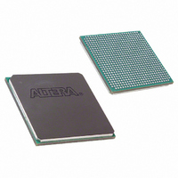
EP2S15F672C3 Altera, EP2S15F672C3 Datasheet - Page 84

EP2S15F672C3
Manufacturer Part Number
EP2S15F672C3
Description
IC STRATIX II FPGA 15K 672-FBGA
Manufacturer
Altera
Series
Stratix® IIr
Datasheet
1.EP2S15F484I4N.pdf
(238 pages)
Specifications of EP2S15F672C3
Number Of Logic Elements/cells
15600
Number Of Labs/clbs
780
Total Ram Bits
419328
Number Of I /o
366
Voltage - Supply
1.15 V ~ 1.25 V
Mounting Type
Surface Mount
Operating Temperature
0°C ~ 85°C
Package / Case
672-FBGA
Lead Free Status / RoHS Status
Contains lead / RoHS non-compliant
Number Of Gates
-
Other names
544-1879
EP2S15F672C3
EP2S15F672C3
Available stocks
Company
Part Number
Manufacturer
Quantity
Price
Company:
Part Number:
EP2S15F672C3
Manufacturer:
ALTERA
Quantity:
3 000
Company:
Part Number:
EP2S15F672C3N
Manufacturer:
ALTERA
Quantity:
500
- Current page: 84 of 238
- Download datasheet (3Mb)
I/O Structure
Figure 2–51. Stratix II IOE in Bidirectional I/O Configuration
Notes to
(1)
(2)
2–76
Stratix II Device Handbook, Volume 1
Column, Row,
Interconnect
or Local
All input signals to the IOE can be inverted at the IOE.
The optional PCI clamp is only available on column I/O pins.
ioe_clk[7..0]
Figure
2–51:
clkout
clkin
oe
ce_out
aclr/apreset
ce_in
sclr/spreset
Chip-Wide Reset
Figure 2–51
shows the IOE in bidirectional configuration.
Output Register
Input Register
OE Register
D
ENA
CLRN/PRN
ENA
D
CLRN/PRN
D
CLRN/PRN
ENA
Q
Q
Q
Drive Strength Control
Open-Drain Output
Pin Delay
Note (1)
Output
Input Register Delay
Logic Array Delay
Input Pin to
Input Pin to
OE Register
t
CO
Delay
V
CCIO
PCI Clamp (2)
V
Altera Corporation
CCIO
Bus-Hold
Circuit
Termination
On-Chip
Programmable
Pull-Up
Resistor
May 2007
Related parts for EP2S15F672C3
Image
Part Number
Description
Manufacturer
Datasheet
Request
R

Part Number:
Description:
CYCLONE II STARTER KIT EP2C20N
Manufacturer:
Altera
Datasheet:

Part Number:
Description:
CPLD, EP610 Family, ECMOS Process, 300 Gates, 16 Macro Cells, 16 Reg., 16 User I/Os, 5V Supply, 35 Speed Grade, 24DIP
Manufacturer:
Altera Corporation
Datasheet:

Part Number:
Description:
CPLD, EP610 Family, ECMOS Process, 300 Gates, 16 Macro Cells, 16 Reg., 16 User I/Os, 5V Supply, 15 Speed Grade, 24DIP
Manufacturer:
Altera Corporation
Datasheet:

Part Number:
Description:
Manufacturer:
Altera Corporation
Datasheet:

Part Number:
Description:
CPLD, EP610 Family, ECMOS Process, 300 Gates, 16 Macro Cells, 16 Reg., 16 User I/Os, 5V Supply, 30 Speed Grade, 24DIP
Manufacturer:
Altera Corporation
Datasheet:

Part Number:
Description:
High-performance, low-power erasable programmable logic devices with 8 macrocells, 10ns
Manufacturer:
Altera Corporation
Datasheet:

Part Number:
Description:
High-performance, low-power erasable programmable logic devices with 8 macrocells, 7ns
Manufacturer:
Altera Corporation
Datasheet:

Part Number:
Description:
Classic EPLD
Manufacturer:
Altera Corporation
Datasheet:

Part Number:
Description:
High-performance, low-power erasable programmable logic devices with 8 macrocells, 10ns
Manufacturer:
Altera Corporation
Datasheet:

Part Number:
Description:
Manufacturer:
Altera Corporation
Datasheet:

Part Number:
Description:
Manufacturer:
Altera Corporation
Datasheet:

Part Number:
Description:
Manufacturer:
Altera Corporation
Datasheet:

Part Number:
Description:
CPLD, EP610 Family, ECMOS Process, 300 Gates, 16 Macro Cells, 16 Reg., 16 User I/Os, 5V Supply, 25 Speed Grade, 24DIP
Manufacturer:
Altera Corporation
Datasheet:


