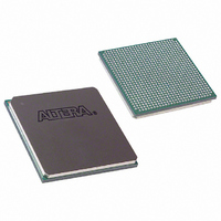
EP2SGX30DF780C5N Altera, EP2SGX30DF780C5N Datasheet - Page 252

EP2SGX30DF780C5N
Manufacturer Part Number
EP2SGX30DF780C5N
Description
IC STRATIX II GX 30K 780-FBGA
Manufacturer
Altera
Series
Stratix® II GXr
Datasheet
1.EP2SGX30DF780C5.pdf
(316 pages)
Specifications of EP2SGX30DF780C5N
Number Of Logic Elements/cells
33880
Number Of Labs/clbs
1694
Total Ram Bits
1369728
Number Of I /o
361
Voltage - Supply
1.15 V ~ 1.25 V
Mounting Type
Surface Mount
Operating Temperature
0°C ~ 70°C
Package / Case
780-FBGA
Family Name
Stratix II GX
Number Of Logic Blocks/elements
33880
# I/os (max)
361
Frequency (max)
609.76MHz
Process Technology
SRAM
Operating Supply Voltage (typ)
1.2V
Logic Cells
33880
Ram Bits
1369728
Operating Supply Voltage (min)
1.15V
Operating Supply Voltage (max)
1.25V
Operating Temp Range
0C to 85C
Operating Temperature Classification
Commercial
Mounting
Surface Mount
Pin Count
780
Package Type
FC-FBGA
Lead Free Status / RoHS Status
Lead free / RoHS Compliant
Number Of Gates
-
Lead Free Status / Rohs Status
Compliant
Other names
544-1754
Available stocks
Company
Part Number
Manufacturer
Quantity
Price
Part Number:
EP2SGX30DF780C5N
Manufacturer:
ALTERA/阿尔特拉
Quantity:
20 000
- Current page: 252 of 316
- Download datasheet (2Mb)
(1)
(1)
(2)
(3)
Clock skew adder
EP2SGX130
Input
delay from
pin to
internal
cells
Input
delay from
pin to
input
register
Delay
from
output
register to
output pin
Output
enable pin
delay
Parameter
Table 4–79. Clock Network Specifications (Part 2 of 2)
Table 4–80. Stratix II GX IOE Programmable Delay on Column Pins
This is in addition to intra-clock network skew, which is modeled in the Quartus II software.
The incremental values for the settings are generally linear. For the exact delay associated with each setting, use the latest
version of the Quartus II software.
This column refers to –3 speed grades for EP2SGX30, EP2SGX60, and EP2SGX90 devices.
This column refers to –3 speed grades for EP2SGX130 devices.
Name
Pad to
I/O
dataout
to core
Pad to
I/O input
register
I/O
output
register
to pad
t
Affected
XZ
(1)
Paths
, t
ZX
Available
Settings
64
8
2
2
Inter-clock network, same side
Inter-clock network, entire chip
IOE Programmable Delay
See
Tables 4–80
Offset
Min
Minimum
0
0
0
0
Timing
Description
Offset
1781
2053
Max
332
320
and
Offset
Min
Grade
0
0
0
0
4–81
-3 Speed
Offset
2881
3275
for IOE programmable delay.
(2)
Max
500
483
Offset
Min
Grade
-3 Speed
0
0
0
0
Min
Offset
3025
3439
(3)
Max
525
507
Note (1)
-4 Speed Grade
Offset
Typ
Min
0
0
0
0
Offset
3217
3657
Max
559
539
Max
±125
±63
Offset
Min
-5 Speed
0
0
0
0
Grade
Unit
3,860
Offset
ps
ps
4388
Max
670
647
Unit
ps
ps
ps
ps
Related parts for EP2SGX30DF780C5N
Image
Part Number
Description
Manufacturer
Datasheet
Request
R

Part Number:
Description:
CYCLONE II STARTER KIT EP2C20N
Manufacturer:
Altera
Datasheet:

Part Number:
Description:
CPLD, EP610 Family, ECMOS Process, 300 Gates, 16 Macro Cells, 16 Reg., 16 User I/Os, 5V Supply, 35 Speed Grade, 24DIP
Manufacturer:
Altera Corporation
Datasheet:

Part Number:
Description:
CPLD, EP610 Family, ECMOS Process, 300 Gates, 16 Macro Cells, 16 Reg., 16 User I/Os, 5V Supply, 15 Speed Grade, 24DIP
Manufacturer:
Altera Corporation
Datasheet:

Part Number:
Description:
Manufacturer:
Altera Corporation
Datasheet:

Part Number:
Description:
CPLD, EP610 Family, ECMOS Process, 300 Gates, 16 Macro Cells, 16 Reg., 16 User I/Os, 5V Supply, 30 Speed Grade, 24DIP
Manufacturer:
Altera Corporation
Datasheet:

Part Number:
Description:
High-performance, low-power erasable programmable logic devices with 8 macrocells, 10ns
Manufacturer:
Altera Corporation
Datasheet:

Part Number:
Description:
High-performance, low-power erasable programmable logic devices with 8 macrocells, 7ns
Manufacturer:
Altera Corporation
Datasheet:

Part Number:
Description:
Classic EPLD
Manufacturer:
Altera Corporation
Datasheet:

Part Number:
Description:
High-performance, low-power erasable programmable logic devices with 8 macrocells, 10ns
Manufacturer:
Altera Corporation
Datasheet:

Part Number:
Description:
Manufacturer:
Altera Corporation
Datasheet:

Part Number:
Description:
Manufacturer:
Altera Corporation
Datasheet:

Part Number:
Description:
Manufacturer:
Altera Corporation
Datasheet:

Part Number:
Description:
CPLD, EP610 Family, ECMOS Process, 300 Gates, 16 Macro Cells, 16 Reg., 16 User I/Os, 5V Supply, 25 Speed Grade, 24DIP
Manufacturer:
Altera Corporation
Datasheet:


