AT6003-2JC Atmel, AT6003-2JC Datasheet - Page 9
AT6003-2JC
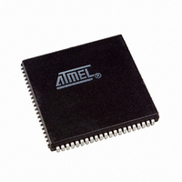
Manufacturer Part Number
AT6003-2JC
Description
IC FPGA 9K GATE 2NS 84PLCC
Manufacturer
Atmel
Series
AT6000(LV)r
Datasheet
1.AT6002-4JC.pdf
(28 pages)
Specifications of AT6003-2JC
Number Of Logic Elements/cells
1600
Number Of I /o
64
Number Of Gates
9000
Voltage - Supply
4.75 V ~ 5.25 V
Mounting Type
Surface Mount
Operating Temperature
0°C ~ 70°C
Package / Case
84-PLCC
Lead Free Status / RoHS Status
Contains lead / RoHS non-compliant
Number Of Labs/clbs
-
Total Ram Bits
-
Other names
AT60032JC
Available stocks
Company
Part Number
Manufacturer
Quantity
Price


The devices can be partially reconfigured while in opera-
tion. Portions of the device not being modified remain
operational during reconfiguration. Simultaneous configu-
ration of more than one device is also possible. Full
configuration takes as little as a millisecond, partial configu-
ration is even faster.
Refer to the Pin Function Description section following for a
brief summary of the pins used in configuration. For more
information about configuration, refer to the AT6000 Series
Configuration data sheet.
Pin Function Description
This section provides abbreviated descriptions of the vari-
ous AT6000 Series pins. For more complete descriptions,
refer to the AT6000 Series Configuration data sheet.
Pinout tables for the AT6000 series of devices follow.
Power Pins
V
V
internal logic supply pins. V
same trace on the printed circuit board. GND and V
should be tied to the same trace on the printed circuit
board.
Input/Output Pins
All I/O pins can be used in the same way (refer to the I/O
section of the architecture description). Some I/O pins are
dual-function pins used during configuration of the array.
When not being used for configuration, dual-function I/Os
are fully functional as normal I/O pins. On initial power-up,
all I/Os are configured as TTL inputs with a pull-up.
Dedicated Timing and Control Pins
CON
Configuration-in-process pin. After power-up, CON stay-
sLow until power-up initialization is complete, at which time
CON is then released. CON is an open collector signal.
After power-up initialization, forcing CON low begins the
configuration process.
CS
Configuration enable pin. All configuration pins are ignored
if CS is high. CS must be held low throughout the configu-
ration process. CS is a TTL input pin.
CC
CC
, V
and GND are the I/O supply pins, V
DD
, GND, V
SS
CC
and V
DD
should be tied to the
DD
and V
SS
are the
SS
M0, M1, M2
Configuration mode pins are used to determine the config-
uration mode. All three are TTL input pins.
CCLK
Configuration clock pin. CCLK is a TTL input or a CMOS
output depending on the mode of operation. In modes 1, 2,
3, and 6 it is an input. In modes 4 and 5 it is an output with
a typical frequency of 1 MHz. In all modes, the rising edge
of the CCLK signal is used to sample inputs and change
outputs.
CLOCK
External logic source used to drive the internal global clock
line. Registers toggle on the rising edge of CLOCK. The
CLOCK signal is neither used nor affected by the configu-
ration modes. It is always a TTL input.
RESET
Array register asynchronous reset. RESET drives the inter-
nal global reset. The RESET signal is neither used nor
affected by the configuration modes. It is always a TTL
input.
Dual-function Pins
When CON is high, dual-function I/O pins act as device
I/Os; when CON is low, dual-function pins are used as con-
figuration control or data signals as determined by the
configuration modes. Care must be taken when using
these pins to ensure that configuration activity does not
interfere with other circuitry connected to these pins in the
application.
D0 or I/O
Serial configuration modes use D0 as the serial data input
pin. Parallel configuration modes use D0 as the least-sig-
ni fic an t bi t. Inpu t d ata mus t mee t s etu p a nd hol d
requirements with respect to the rising edge of CCLK. D0 is
a TTL input during configuration.
D1 to D7 or I/O
Parallel configuration modes use these pins as inputs.
Serial configuration modes do not use them. Data must
meet setup and hold requirements with respect to the rising
edge of CCLK. D1 - D7 are TTL inputs during configuration.
A0 to A16 or I/O
During configuration in modes 1, 2 and 5, these pins are
CMOS outputs and act as the address pins for a parallel
EPROM. A0 - A16 eliminates the need for an external
address counter when using an external parallel nonvolatile
AT6000(LV) Series
9
Related parts for AT6003-2JC
Image
Part Number
Description
Manufacturer
Datasheet
Request
R

Part Number:
Description:
IC FPGA 2NS 132BQFP
Manufacturer:
Atmel
Datasheet:

Part Number:
Description:
IC FPGA 9K GATE 4NS 100VQFP
Manufacturer:
Atmel
Datasheet:

Part Number:
Description:
IC FPGA 4NS 84PLCC
Manufacturer:
Atmel
Datasheet:
Part Number:
Description:
IC FPGA 9K GATE 2NS 100VQFP
Manufacturer:
Atmel
Datasheet:
Part Number:
Description:
IC FPGA 2NS 84PLCC
Manufacturer:
Atmel
Datasheet:
Part Number:
Description:
IC FPGA 9K GATE 4NS 100VQFP
Manufacturer:
Atmel
Datasheet:
Part Number:
Description:
IC FPGA 2NS 100VQFP
Manufacturer:
Atmel
Datasheet:
Part Number:
Description:
IC FPGA 9K GATE 2NS 132BQFP
Manufacturer:
Atmel
Datasheet:
Part Number:
Description:
IC FPGA 9K GATE 4NS 132BQFP
Manufacturer:
Atmel
Datasheet:
Part Number:
Description:
IC FPGA 9K GATE 4NS 132BQFP
Manufacturer:
Atmel
Datasheet:
Part Number:
Description:
FPGA - Field Programmable Gate Array ASICS
Manufacturer:
Atmel
Datasheet:

Part Number:
Description:
CONN PIN 14-16AWG SIZE 16 NICKEL
Manufacturer:
Amphenol Sine Systems Corp
Datasheet:

Part Number:
Description:
CONN PIN 16-18AWG SIZE 16 NICKEL
Manufacturer:
Amphenol Sine Systems Corp
Datasheet:

Part Number:
Description:
CONN PIN 12-14AWG GOLD
Manufacturer:
Amphenol Sine Systems Corp
Datasheet:

Part Number:
Description:
CONN MALE 18-20AWG NICKEL PLATE
Manufacturer:
Amphenol Sine Systems Corp
Datasheet: