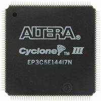
EP3C5E144I7N Altera, EP3C5E144I7N Datasheet - Page 125

EP3C5E144I7N
Manufacturer Part Number
EP3C5E144I7N
Description
IC CYCLONE III FPGA 5K 144 EQFP
Manufacturer
Altera
Series
Cyclone® IIIr
Datasheets
1.EP3C5F256C8N.pdf
(5 pages)
2.EP3C5F256C8N.pdf
(34 pages)
3.EP3C5F256C8N.pdf
(66 pages)
4.EP3C5F256C8N.pdf
(14 pages)
5.EP3C5F256C8N.pdf
(76 pages)
6.EP3C5E144I7N.pdf
(274 pages)
Specifications of EP3C5E144I7N
Number Of Logic Elements/cells
5136
Number Of Labs/clbs
321
Total Ram Bits
423936
Number Of I /o
94
Voltage - Supply
1.15 V ~ 1.25 V
Mounting Type
Surface Mount
Operating Temperature
-40°C ~ 100°C
Package / Case
144-EQFP
Family Name
Cyclone III
Number Of Logic Blocks/elements
5136
# I/os (max)
94
Frequency (max)
437.5MHz
Process Technology
65nm
Operating Supply Voltage (typ)
1.2V
Logic Cells
5136
Ram Bits
423936
Operating Supply Voltage (min)
1.15V
Operating Supply Voltage (max)
1.25V
Operating Temp Range
-40C to 100C
Operating Temperature Classification
Industrial
Mounting
Surface Mount
Pin Count
144
Package Type
EQFP
For Use With
544-2601 - KIT DEV CYCLONE III LS EP3CLS200544-2411 - KIT DEV NIOS II CYCLONE III ED.
Lead Free Status / RoHS Status
Lead free / RoHS Compliant
Number Of Gates
-
Lead Free Status / Rohs Status
Compliant
Other names
544-2557
Available stocks
Company
Part Number
Manufacturer
Quantity
Price
Company:
Part Number:
EP3C5E144I7N
Manufacturer:
Altera
Quantity:
135
Company:
Part Number:
EP3C5E144I7N
Manufacturer:
ALTERA32
Quantity:
345
Part Number:
EP3C5E144I7N
Manufacturer:
ALTERA/阿尔特拉
Quantity:
20 000
High-Speed I/O Interface
© December 2009
CIII51008-3.2
f
Altera Corporation
This chapter describes the high-speed differential I/O features and resources in the
Cyclone III device family.
High-speed differential I/O standards have become popular in high-speed interfaces
because of their significant advantages over single-ended I/O standards. The Altera
Cyclone
BLVDS, reduced swing differential signaling (RSDS), mini-LVDS, and point-to-point
differential signaling (PPDS).
This chapter contains the following sections:
■
■
■
■
■
■
Cyclone III device family I/Os are separated into eight I/O banks, as shown in
Figure
LVDS, RSDS, mini-LVDS, and PPDS are on the left and right I/O banks. These I/O
standards are also supported on the top and bottom I/O banks using external
resistors. On the left and right I/O banks, some of the differential pin pairs (p and n
pins) of the true output drivers are not located on adjacent pins. In these cases, a
power pin is located between the p and n pins. These I/O standards are also
supported on all I/O banks using two single-ended output with the second output
programmed as inverted, and an external resistor network. True input buffers for
these I/O standards are supported on all I/O banks.
For more information about the location of Cyclone III device family true differential
pins, refer to the
“High-Speed I/O Interface” on page 7–1
“High-Speed I/O Standards Support” on page 7–7
“True Output Buffer Feature” on page 7–15
“High-Speed I/O Timing” on page 7–16
“Design Guidelines” on page 7–17
“Software Overview” on page 7–18
7–1. Each bank has an independent power supply. True output drivers for
®
III device family (Cyclone III and Cyclone III LS devices) supports LVDS,
Cyclone III Devices Pin-Outs
7. High-Speed Differential Interfaces in
the Cyclone III Device Family
on the Altera website.
Cyclone III Device Handbook, Volume 1
®


