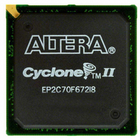
EP2C70F672I8 Altera, EP2C70F672I8 Datasheet - Page 120

EP2C70F672I8
Manufacturer Part Number
EP2C70F672I8
Description
IC CYCLONE II FPGA 70K 672-FBGA
Manufacturer
Altera
Series
Cyclone® IIr
Datasheet
1.EP2C5T144C8N.pdf
(168 pages)
Specifications of EP2C70F672I8
Number Of Logic Elements/cells
68416
Number Of Labs/clbs
4276
Total Ram Bits
1152000
Number Of I /o
422
Voltage - Supply
1.15 V ~ 1.25 V
Mounting Type
Surface Mount
Operating Temperature
-40°C ~ 100°C
Package / Case
672-FBGA
For Use With
P0304 - DE2-70 CALL FOR ACADEMIC PRICING544-1703 - VIDEO KIT W/CYCLONE II EP2C70N544-1699 - DSP KIT W/CYCLONE II EPS2C70N
Lead Free Status / RoHS Status
Contains lead / RoHS non-compliant
Number Of Gates
-
Other names
544-2142
Available stocks
Company
Part Number
Manufacturer
Quantity
Price
Company:
Part Number:
EP2C70F672I8
Manufacturer:
ALTERA
Quantity:
288
Company:
Part Number:
EP2C70F672I8
Manufacturer:
ALTERA
Quantity:
325
Company:
Part Number:
EP2C70F672I8N
Manufacturer:
ALTERA
Quantity:
490
Part Number:
EP2C70F672I8N
Manufacturer:
BGA
Quantity:
20 000
Timing Specifications
5–30
Cyclone II Device Handbook, Volume 1
Notes to
(1)
(2)
(3)
(4)
Input Delay
from Pin to
Internal
Cells
Input Delay
from Pin to
Input
Register
Delay from
Output
Register to
Output Pin
Input Delay
from Pin to
Internal
Cells
Parameter
Parameter Paths Affected
Table 5–36. Cyclone II IOE Programmable Delay on Column Pins
Table 5–37. Cyclone II IOE Programmable Delay on Row Pins
The incremental values for the settings are generally linear. For exact values of each setting, use the latest version
of the Quartus II software.
The minimum and maximum offset timing numbers are in reference to setting “0” as available in the Quartus II
software.
The value in the first row for each parameter represents the fast corner timing parameter for industrial and
automotive devices. The second row represents the fast corner timing parameter for commercial devices.
The value in the first row is for automotive devices. The second row is for commercial devices.
Table
Pad ->
I/O
dataout
to core
Pad -> I/O
dataout to core
Pad -> I/O
input register
I/O output
register -> Pad
Affected
Paths
5–36:
Settings
Number
of
7
IOE Programmable Delay
Refer to
Settings
Number
of
7
8
2
Fast Corner
Offset
Min
0
0
Table 5–36
Offset
Fast Corner
Min
0
0
0
0
0
0
Offset
2240
2352
Max
(3)
(3)
Offset
2233
2344
2656
2788
Max
303
318
and
Offset
Min
—
0
–6 Speed
5–37
Offset
Grade
Min
—
—
—
–6 Speed
0
0
0
Grade
Offset
for IOE programmable delay.
3776
Max
—
Offset
3827
4555
Notes
Max
563
—
—
—
Notes
Offset
Min
(1),
Offset
0
0
–7 Speed
Grade
Min
–7 Speed
0
0
0
0
0
0
(1),
(2)
Grade
(4)
Offset
(4)
4174
4033
(2)
Max
(Part 1 of 2)
Offset
4232
4088
4914
4748
Max
638
617
–8 Speed Grade
Offset
Offset
Min
Min
—
—
—
—
0
Altera Corporation
–8 Speed
0
0
0
Grade
February 2008
Offset
Offset
4349
4940
4290
Max
Max
670
—
—
—
—
Unit
Unit
ps
ps
ps
ps
ps
ps
ps
ps


