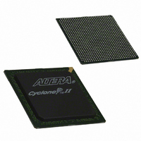
EP2C70F896C7 Altera, EP2C70F896C7 Datasheet - Page 73

EP2C70F896C7
Manufacturer Part Number
EP2C70F896C7
Description
IC CYCLONE II FPGA 70K 896-FBGA
Manufacturer
Altera
Series
Cyclone® IIr
Datasheet
1.EP2C5T144C8N.pdf
(168 pages)
Specifications of EP2C70F896C7
Number Of Logic Elements/cells
68416
Number Of Labs/clbs
4276
Total Ram Bits
1152000
Number Of I /o
622
Voltage - Supply
1.15 V ~ 1.25 V
Mounting Type
Surface Mount
Operating Temperature
0°C ~ 85°C
Package / Case
896-FBGA
For Use With
P0304 - DE2-70 CALL FOR ACADEMIC PRICING544-1703 - VIDEO KIT W/CYCLONE II EP2C70N544-1699 - DSP KIT W/CYCLONE II EPS2C70N
Lead Free Status / RoHS Status
Contains lead / RoHS non-compliant
Number Of Gates
-
Other names
544-1452
Available stocks
Company
Part Number
Manufacturer
Quantity
Price
Part Number:
EP2C70F896C7
Manufacturer:
ALTERA/阿尔特拉
Quantity:
20 000
Company:
Part Number:
EP2C70F896C7N
Manufacturer:
ALTERA
Quantity:
3
Altera Corporation
February 2007
Notes to
(1)
(2)
(3)
(4)
(5)
(6)
Table 2–20. Cyclone II MultiVolt I/O Support (Part 2 of 2)
V
CCIO
3.3
The PCI clamping diode must be disabled to drive an input with voltages higher than V
These input values overdrive the input buffer, so the pin leakage current is slightly higher than the default value.
To drive inputs higher than V
overdrive for LVTTL/LVCMOS input pins option in Device setting option in the Quartus II software.
When V
When V
feeds an input pin, the V
that the input signal level does not drive to the V
When V
When V
(V)
Table
CCIO
CCIO
CCIO
CCIO
2–20:
1.5 V
= 1.8-V, a Cyclone II device can drive a 1.5-V device with 1.8-V tolerant inputs.
= 3.3-V and a 2.5-V input signal feeds an input pin or when V
= 2.5-V, a Cyclone II device can drive a 1.5-V or 1.8-V device with 2.5-V tolerant inputs.
= 3.3-V, a Cyclone II device can drive a 1.5-V, 1.8-V, or 2.5-V device with 3.3-V tolerant inputs.
1.8 V
CCIO
Input Signal
supply current will be slightly larger than expected. The reason for this increase is
CCIO
but less than 4.0 V, disable the PCI clamping diode and turn on Allow voltage
v
2.5 V
(4)
CCIO
3.3 V
v
rail, which causes the input buffer to not completely shut off.
v
Note (1)
1.5 V
(6)
Cyclone II Device Handbook, Volume 1
C C I O
v
1.8 V
Output Signal
= 1.8-V and a 1.5-V input signal
(6)
Cyclone II Architecture
CCIO
v
2.5 V
.
(6)
3.3 V
v
2–61


