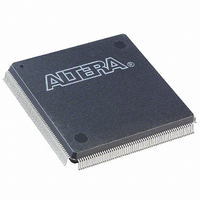
EPF10K100EQC240-1N Altera, EPF10K100EQC240-1N Datasheet - Page 50

EPF10K100EQC240-1N
Manufacturer Part Number
EPF10K100EQC240-1N
Description
IC FLEX 10KE FPGA 100K 240-PQFP
Manufacturer
Altera
Series
FLEX-10KE®r
Datasheet
1.EPF10K30ETC144-3.pdf
(100 pages)
Specifications of EPF10K100EQC240-1N
Number Of Logic Elements/cells
4992
Number Of Labs/clbs
624
Total Ram Bits
49152
Number Of I /o
189
Number Of Gates
257000
Voltage - Supply
2.375 V ~ 2.625 V
Mounting Type
Surface Mount
Operating Temperature
0°C ~ 85°C
Package / Case
240-MQFP, 240-PQFP
Lead Free Status / RoHS Status
Lead free / RoHS Compliant
Available stocks
Company
Part Number
Manufacturer
Quantity
Price
Part Number:
EPF10K100EQC240-1N
Manufacturer:
ALTERA
Quantity:
20 000
FLEX 10KE Embedded Programmable Logic Devices Data Sheet
Notes to tables:
(1)
(2)
(3)
(4)
(5)
(6)
(7)
(8)
(9)
(10) The I
(11) This value is specified for normal device operation. The value may vary during power-up.
(12) This parameter applies to -1 speed-grade commercial-temperature devices and -2 speed-grade-industrial
(13) Pin pull-up resistance values will be lower if the pin is driven higher than V
(14) Capacitance is sample-tested only.
50
Symbol
C
C
C
Table 23. FLEX 10KE Device Capacitance
IN
INCLK
OUT
See the
Minimum DC input voltage is –0.5 V. During transitions, the inputs may undershoot to –2.0 V for input currents
less than 100 mA and periods shorter than 20 ns.
Numbers in parentheses are for industrial-temperature-range devices.
Maximum V
All pins, including dedicated inputs, clock, I/O, and JTAG pins, may be driven before V
powered.
Typical values are for T
These values are specified under the FLEX 10KE Recommended Operating Conditions shown in
The FLEX 10KE input buffers are compatible with 2.5-V, 3.3-V (LVTTL and LVCMOS), and 5.0-V TTL and CMOS
signals. Additionally, the input buffers are 3.3-V PCI compliant when
in
The I
as well as output pins.
temperature devices.
Figure
OL
OH
Input capacitance
Input capacitance on
dedicated clock pin
Output capacitance
Operating Requirements for Altera Devices Data
parameter refers to low-level TTL, PCI, or CMOS output current. This parameter applies to open-drain pins
parameter refers to high-level TTL, PCI, or CMOS output current.
22.
CC
Parameter
rise time is 100 ms, and V
A
= 25 C, V
CCINT
V
V
V
IN
IN
OUT
CC
= 0 V, f = 1.0 MHz
= 0 V, f = 1.0 MHz
= 2.5 V, and V
= 0 V, f = 1.0 MHz
must rise monotonically.
Note (14)
Conditions
Sheet.
CCIO
= 2.5 V or 3.3 V.
V
CCIO
and V
CCIO
CCINT
Min
by an external source.
meet the relationship shown
CCINT
Max
Altera Corporation
10
12
10
and V
Tables 20
CCIO
Unit
are
pF
pF
pF
and 21.


