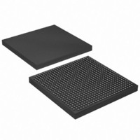
EP1S25F672C8N Altera, EP1S25F672C8N Datasheet - Page 154

EP1S25F672C8N
Manufacturer Part Number
EP1S25F672C8N
Description
IC STRATIX FPGA 25K LE 672-FBGA
Manufacturer
Altera
Series
Stratix®r
Datasheet
1.EP1S10F780C7.pdf
(276 pages)
Specifications of EP1S25F672C8N
Number Of Logic Elements/cells
25660
Number Of Labs/clbs
2566
Total Ram Bits
1944576
Number Of I /o
473
Voltage - Supply
1.425 V ~ 1.575 V
Mounting Type
Surface Mount
Operating Temperature
0°C ~ 85°C
Package / Case
672-FBGA
Lead Free Status / RoHS Status
Lead free / RoHS Compliant
Number Of Gates
-
Available stocks
Company
Part Number
Manufacturer
Quantity
Price
Company:
Part Number:
EP1S25F672C8N
Manufacturer:
ALTERA
Quantity:
465
Part Number:
EP1S25F672C8N
Manufacturer:
ALTERA/阿尔特拉
Quantity:
20 000
- Current page: 154 of 276
- Download datasheet (4Mb)
Power Sequencing & Hot Socketing
Power
Sequencing &
Hot Socketing
2–140
Stratix Device Handbook, Volume 1
The transmitter external clock output is transmitted on a data channel.
The txclk pin for each bank is located in between data transmitter pins.
For ×1 clocks (e.g., 622 Mbps, 622 MHz), the high-speed PLL clock
bypasses the SERDES to drive the output pins. For half-rate clocks (e.g.,
622 Mbps, 311 MHz) or any other even-numbered factor such as 1/4, 1/7,
1/8, or 1/10, the SERDES automatically generates the clock in the
Quartus II software.
For systems that require more than four or eight high-speed differential
I/O clock domains, a SERDES bypass implementation is possible using
IOEs.
Byte Alignment
For high-speed source synchronous interfaces such as POS-PHY 4, XSBI,
RapidIO, and HyperTransport technology, the source synchronous clock
rate is not a byte- or SERDES-rate multiple of the data rate. Byte
alignment is necessary for these protocols since the source synchronous
clock does not provide a byte or word boundary since the clock is one half
the data rate, not one eighth. The Stratix device’s high-speed differential
I/O circuitry provides dedicated data realignment circuitry for user-
controlled byte boundary shifting. This simplifies designs while saving
LE resources. An input signal to each fast PLL can stall deserializer
parallel data outputs by one bit period. You can use an LE-based state
machine to signal the shift of receiver byte boundaries until a specified
pattern is detected to indicate byte alignment.
Because Stratix devices can be used in a mixed-voltage environment, they
have been designed specifically to tolerate any possible power-up
sequence. Therefore, the VCCIO and VCCINT power supplies may be
powered in any order.
Although you can power up or down the VCCIO and VCCINT power
supplies in any sequence, you should not power down any I/O banks
that contain configuration pins while leaving other I/O banks powered
on. For power up and power down, all supplies (VCCINT and all VCCIO
power planes) must be powered up and down within 100 ms of each
other. This prevents I/O pins from driving out.
Signals can be driven into Stratix devices before and during power up
without damaging the device. In addition, Stratix devices do not drive
out during power up. Once operating conditions are reached and the
device is configured, Stratix devices operate as specified by the user. For
more information, see Hot Socketing in the Selectable I/O Standards in
Stratix & Stratix GX Devices chapter in the Stratix Device Handbook,
Volume 2.
Altera Corporation
July 2005
Related parts for EP1S25F672C8N
Image
Part Number
Description
Manufacturer
Datasheet
Request
R

Part Number:
Description:
CYCLONE II STARTER KIT EP2C20N
Manufacturer:
Altera
Datasheet:

Part Number:
Description:
CPLD, EP610 Family, ECMOS Process, 300 Gates, 16 Macro Cells, 16 Reg., 16 User I/Os, 5V Supply, 35 Speed Grade, 24DIP
Manufacturer:
Altera Corporation
Datasheet:

Part Number:
Description:
CPLD, EP610 Family, ECMOS Process, 300 Gates, 16 Macro Cells, 16 Reg., 16 User I/Os, 5V Supply, 15 Speed Grade, 24DIP
Manufacturer:
Altera Corporation
Datasheet:

Part Number:
Description:
Manufacturer:
Altera Corporation
Datasheet:

Part Number:
Description:
CPLD, EP610 Family, ECMOS Process, 300 Gates, 16 Macro Cells, 16 Reg., 16 User I/Os, 5V Supply, 30 Speed Grade, 24DIP
Manufacturer:
Altera Corporation
Datasheet:

Part Number:
Description:
High-performance, low-power erasable programmable logic devices with 8 macrocells, 10ns
Manufacturer:
Altera Corporation
Datasheet:

Part Number:
Description:
High-performance, low-power erasable programmable logic devices with 8 macrocells, 7ns
Manufacturer:
Altera Corporation
Datasheet:

Part Number:
Description:
Classic EPLD
Manufacturer:
Altera Corporation
Datasheet:

Part Number:
Description:
High-performance, low-power erasable programmable logic devices with 8 macrocells, 10ns
Manufacturer:
Altera Corporation
Datasheet:

Part Number:
Description:
Manufacturer:
Altera Corporation
Datasheet:

Part Number:
Description:
Manufacturer:
Altera Corporation
Datasheet:

Part Number:
Description:
Manufacturer:
Altera Corporation
Datasheet:

Part Number:
Description:
CPLD, EP610 Family, ECMOS Process, 300 Gates, 16 Macro Cells, 16 Reg., 16 User I/Os, 5V Supply, 25 Speed Grade, 24DIP
Manufacturer:
Altera Corporation
Datasheet:


