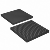
EP1S20F672C6 Altera, EP1S20F672C6 Datasheet - Page 104

EP1S20F672C6
Manufacturer Part Number
EP1S20F672C6
Description
IC STRATIX FPGA 20K LE 672-FBGA
Manufacturer
Altera
Series
Stratix®r
Datasheet
1.EP1S10F780C7.pdf
(276 pages)
Specifications of EP1S20F672C6
Number Of Logic Elements/cells
18460
Number Of Labs/clbs
1846
Total Ram Bits
1669248
Number Of I /o
426
Voltage - Supply
1.425 V ~ 1.575 V
Mounting Type
Surface Mount
Operating Temperature
0°C ~ 85°C
Package / Case
672-FBGA
Lead Free Status / RoHS Status
Contains lead / RoHS non-compliant
Number Of Gates
-
Other names
544-1853
EP1S20F672C6
EP1S20F672C6
Available stocks
Company
Part Number
Manufacturer
Quantity
Price
Company:
Part Number:
EP1S20F672C6
Manufacturer:
ALTERA
Quantity:
528
Part Number:
EP1S20F672C6N
Manufacturer:
ALTERA/阿尔特拉
Quantity:
20 000
- Current page: 104 of 276
- Download datasheet (4Mb)
PLLs & Clock Networks
2–90
Stratix Device Handbook, Volume 1
f
During switchover, the PLL VCO continues to run and will either slow
down or speed up, generating frequency drift on the PLL outputs. The
clock switchover transitions without any glitches. After the switch, there
is a finite resynchronization period to lock onto new clock as the VCO
ramps up. The exact amount of time it takes for the PLL to relock relates
to the PLL configuration and may be adjusted by using the
programmable bandwidth feature of the PLL. The specification for the
maximum time to relock is 100 µs.
For more information on clock switchover, see AN 313, Implementing
Clock Switchover in Stratix & Stratix GX Devices.
PLL Reconfiguration
The PLL reconfiguration feature enables system logic to change Stratix
device enhanced PLL counters and delay elements without reloading a
Programmer Object File (.pof). This provides considerable flexibility for
frequency synthesis, allowing real-time PLL frequency and output clock
delay variation. You can sweep the PLL output frequencies and clock
delay in prototype environments. The PLL reconfiguration feature can
also dynamically or intelligently control system clock speeds or t
delays in end systems.
Clock delay elements at each PLL output port implement variable delay.
Figure 2–54
for the counters and the clock delay elements. The configuration time is
less than 20 μs for the enhanced PLL using a input shift clock rate of
22 MHz. The charge pump, loop filter components, and phase shifting
using VCO phase taps cannot be dynamically adjusted.
shows a diagram of the overall dynamic PLL control feature
Altera Corporation
July 2005
CO
Related parts for EP1S20F672C6
Image
Part Number
Description
Manufacturer
Datasheet
Request
R

Part Number:
Description:
CYCLONE II STARTER KIT EP2C20N
Manufacturer:
Altera
Datasheet:

Part Number:
Description:
CPLD, EP610 Family, ECMOS Process, 300 Gates, 16 Macro Cells, 16 Reg., 16 User I/Os, 5V Supply, 35 Speed Grade, 24DIP
Manufacturer:
Altera Corporation
Datasheet:

Part Number:
Description:
CPLD, EP610 Family, ECMOS Process, 300 Gates, 16 Macro Cells, 16 Reg., 16 User I/Os, 5V Supply, 15 Speed Grade, 24DIP
Manufacturer:
Altera Corporation
Datasheet:

Part Number:
Description:
Manufacturer:
Altera Corporation
Datasheet:

Part Number:
Description:
CPLD, EP610 Family, ECMOS Process, 300 Gates, 16 Macro Cells, 16 Reg., 16 User I/Os, 5V Supply, 30 Speed Grade, 24DIP
Manufacturer:
Altera Corporation
Datasheet:

Part Number:
Description:
High-performance, low-power erasable programmable logic devices with 8 macrocells, 10ns
Manufacturer:
Altera Corporation
Datasheet:

Part Number:
Description:
High-performance, low-power erasable programmable logic devices with 8 macrocells, 7ns
Manufacturer:
Altera Corporation
Datasheet:

Part Number:
Description:
Classic EPLD
Manufacturer:
Altera Corporation
Datasheet:

Part Number:
Description:
High-performance, low-power erasable programmable logic devices with 8 macrocells, 10ns
Manufacturer:
Altera Corporation
Datasheet:

Part Number:
Description:
Manufacturer:
Altera Corporation
Datasheet:

Part Number:
Description:
Manufacturer:
Altera Corporation
Datasheet:

Part Number:
Description:
Manufacturer:
Altera Corporation
Datasheet:

Part Number:
Description:
CPLD, EP610 Family, ECMOS Process, 300 Gates, 16 Macro Cells, 16 Reg., 16 User I/Os, 5V Supply, 25 Speed Grade, 24DIP
Manufacturer:
Altera Corporation
Datasheet:


