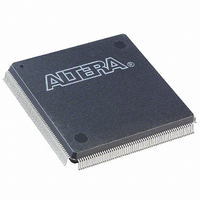
EPF10K130EQI240-2 Altera, EPF10K130EQI240-2 Datasheet - Page 44

EPF10K130EQI240-2
Manufacturer Part Number
EPF10K130EQI240-2
Description
IC FLEX 10KE FPGA 130K 240-PQFP
Manufacturer
Altera
Series
FLEX-10KE®r
Datasheet
1.EPF10K30ETC144-3.pdf
(100 pages)
Specifications of EPF10K130EQI240-2
Number Of Logic Elements/cells
6656
Number Of Labs/clbs
832
Total Ram Bits
65536
Number Of I /o
186
Number Of Gates
342000
Voltage - Supply
2.375 V ~ 2.625 V
Mounting Type
Surface Mount
Operating Temperature
-40°C ~ 100°C
Package / Case
240-MQFP, 240-PQFP
Family Name
FLEX 10KE
Number Of Usable Gates
130000
Number Of Logic Blocks/elements
6656
# Registers
186
# I/os (max)
186
Frequency (max)
333.33MHz
Process Technology
CMOS
Operating Supply Voltage (typ)
2.5V
Logic Cells
6656
Ram Bits
65536
Device System Gates
342000
Operating Supply Voltage (min)
2.375V
Operating Supply Voltage (max)
2.625V
Operating Temp Range
-40C to 100C
Operating Temperature Classification
Industrial
Mounting
Surface Mount
Pin Count
240
Package Type
PQFP
Lead Free Status / RoHS Status
Contains lead / RoHS non-compliant
Other names
544-2206
Available stocks
Company
Part Number
Manufacturer
Quantity
Price
Part Number:
EPF10K130EQI240-2
Manufacturer:
ALTERA/阿尔特拉
Quantity:
20 000
FLEX 10KE Embedded Programmable Logic Devices Data Sheet
IEEE Std.
1149.1 (JTAG)
Boundary-Scan
Support
44
SAMPLE/PRELOAD
EXTEST
BYPASS
USERCODE
IDCODE
ICR Instructions
Table 15. FLEX 10KE JTAG Instructions
JTAG Instruction
Allows a snapshot of signals at the device pins to be captured and examined during
normal device operation, and permits an initial data pattern to be output at the device
pins.
Allows the external circuitry and board-level interconnections to be tested by forcing a
test pattern at the output pins and capturing test results at the input pins.
Places the 1-bit bypass register between the TDI and TDO pins, which allows the BST
data to pass synchronously through a selected device to adjacent devices during normal
device operation.
Selects the user electronic signature (USERCODE) register and places it between the
TDI and TDO pins, allowing the USERCODE to be serially shifted out of TDO.
Selects the IDCODE register and places it between TDI and TDO, allowing the IDCODE
to be serially shifted out of TDO.
These instructions are used when configuring a FLEX 10KE device via JTAG ports with
a BitBlaster or ByteBlasterMV download cable, or using a Jam File (.jam) or
Jam Byte-Code File (.jbc) via an embedded processor.
All FLEX 10KE devices provide JTAG BST circuitry that complies with the
IEEE Std. 1149.1-1990 specification. FLEX 10KE devices can also be
configured using the JTAG pins through the BitBlaster or ByteBlasterMV
download cable, or via hardware that uses the Jam
programming and test language. JTAG boundary-scan testing can be
performed before or after configuration, but not during configuration.
FLEX 10KE devices support the JTAG instructions shown in
The instruction register length of FLEX 10KE devices is 10 bits. The
USERCODE register length in FLEX 10KE devices is 32 bits; 7 bits are
determined by the user, and 25 bits are pre-determined.
show the boundary-scan register length and device IDCODE information
for FLEX 10KE devices.
Table 16. FLEX 10KE Boundary-Scan Register Length
EPF10K30E
EPF10K50E
EPF10K50S
EPF10K100E
EPF10K130E
EPF10K200E
EPF10K200S
Device
Description
Boundary-Scan Register Length
1,050
1,308
1,446
TM
690
798
STAPL
Altera Corporation
Tables 16
Table
and
15.
17


