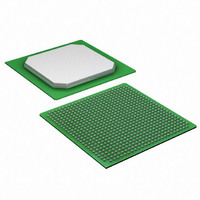
EP1S25B672C7N Altera, EP1S25B672C7N Datasheet - Page 50

EP1S25B672C7N
Manufacturer Part Number
EP1S25B672C7N
Description
IC STRATIX FPGA 25K LE 672-BGA
Manufacturer
Altera
Series
Stratix®r
Datasheet
1.EP1S10F780C7.pdf
(276 pages)
Specifications of EP1S25B672C7N
Number Of Logic Elements/cells
25660
Number Of Labs/clbs
2566
Total Ram Bits
1944576
Number Of I /o
473
Voltage - Supply
1.425 V ~ 1.575 V
Mounting Type
Surface Mount
Operating Temperature
0°C ~ 85°C
Package / Case
672-BGA
Lead Free Status / RoHS Status
Lead free / RoHS Compliant
Number Of Gates
-
Available stocks
Company
Part Number
Manufacturer
Quantity
Price
- Current page: 50 of 276
- Download datasheet (4Mb)
TriMatrix Memory
2–36
Stratix Device Handbook, Volume 1
Similar to all RAM blocks, M-RAM blocks can have different clocks on
their inputs and outputs. All input registers—renwe, datain, address,
and byte enable registers—are clocked together from either of the two
clocks feeding the block. The output register can be bypassed. The eight
labclk signals or local interconnect can drive the control signals for the
A and B ports of the M-RAM block. LEs can also control the clock_a,
clock_b, renwe_a, renwe_b, clr_a, clr_b, clocken_a, and
clocken_b signals as shown in
Notes to
(1)
(2)
Table 2–11. M-RAM Combined Byte Selection for ×144 Mode
Any combination of byte enables is possible.
Byte enables can be used in the same manner with 8-bit words, i.e., in × 16, × 32,
× 64, and × 128 modes.
Tables 2–10
byteena[15..0]
[10] = 1
[11] = 1
[12] = 1
[13] = 1
[14] = 1
[15] = 1
[0] = 1
[1] = 1
[2] = 1
[3] = 1
[4] = 1
[5] = 1
[6] = 1
[7] = 1
[8] = 1
[9] = 1
and 2–11:
Figure
2–19.
datain ×144
[116..108]
[125..117]
[134..126]
[143..135]
[107..99]
[26..18]
[35..27]
[44..36]
[53..45]
[62..54]
[71..63]
[80..72]
[89..81]
[98..90]
[17..9]
[8..0]
Altera Corporation
Notes
July 2005
(1),
(2)
Related parts for EP1S25B672C7N
Image
Part Number
Description
Manufacturer
Datasheet
Request
R

Part Number:
Description:
CYCLONE II STARTER KIT EP2C20N
Manufacturer:
Altera
Datasheet:

Part Number:
Description:
CPLD, EP610 Family, ECMOS Process, 300 Gates, 16 Macro Cells, 16 Reg., 16 User I/Os, 5V Supply, 35 Speed Grade, 24DIP
Manufacturer:
Altera Corporation
Datasheet:

Part Number:
Description:
CPLD, EP610 Family, ECMOS Process, 300 Gates, 16 Macro Cells, 16 Reg., 16 User I/Os, 5V Supply, 15 Speed Grade, 24DIP
Manufacturer:
Altera Corporation
Datasheet:

Part Number:
Description:
Manufacturer:
Altera Corporation
Datasheet:

Part Number:
Description:
CPLD, EP610 Family, ECMOS Process, 300 Gates, 16 Macro Cells, 16 Reg., 16 User I/Os, 5V Supply, 30 Speed Grade, 24DIP
Manufacturer:
Altera Corporation
Datasheet:

Part Number:
Description:
High-performance, low-power erasable programmable logic devices with 8 macrocells, 10ns
Manufacturer:
Altera Corporation
Datasheet:

Part Number:
Description:
High-performance, low-power erasable programmable logic devices with 8 macrocells, 7ns
Manufacturer:
Altera Corporation
Datasheet:

Part Number:
Description:
Classic EPLD
Manufacturer:
Altera Corporation
Datasheet:

Part Number:
Description:
High-performance, low-power erasable programmable logic devices with 8 macrocells, 10ns
Manufacturer:
Altera Corporation
Datasheet:

Part Number:
Description:
Manufacturer:
Altera Corporation
Datasheet:

Part Number:
Description:
Manufacturer:
Altera Corporation
Datasheet:

Part Number:
Description:
Manufacturer:
Altera Corporation
Datasheet:

Part Number:
Description:
CPLD, EP610 Family, ECMOS Process, 300 Gates, 16 Macro Cells, 16 Reg., 16 User I/Os, 5V Supply, 25 Speed Grade, 24DIP
Manufacturer:
Altera Corporation
Datasheet:


