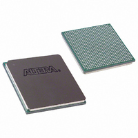
EP1S40F780C8 Altera, EP1S40F780C8 Datasheet - Page 245

EP1S40F780C8
Manufacturer Part Number
EP1S40F780C8
Description
IC STRATIX FPGA 40K LE 780-FBGA
Manufacturer
Altera
Series
Stratix®r
Datasheet
1.EP1S10F780C7.pdf
(276 pages)
Specifications of EP1S40F780C8
Number Of Logic Elements/cells
41250
Number Of Labs/clbs
4125
Total Ram Bits
3423744
Number Of I /o
615
Voltage - Supply
1.425 V ~ 1.575 V
Mounting Type
Surface Mount
Operating Temperature
0°C ~ 85°C
Package / Case
780-FBGA
Lead Free Status / RoHS Status
Contains lead / RoHS non-compliant
Number Of Gates
-
Other names
544-1430
EP1S40SF780C8
EP1S40SF780C8
Available stocks
Company
Part Number
Manufacturer
Quantity
Price
Company:
Part Number:
EP1S40F780C8
Manufacturer:
ALTERA
Quantity:
3 000
Part Number:
EP1S40F780C8
Manufacturer:
ALTERA/阿尔特拉
Quantity:
20 000
Company:
Part Number:
EP1S40F780C8N
Manufacturer:
ALTERA
Quantity:
3 000
- Current page: 245 of 276
- Download datasheet (4Mb)
Altera Corporation
January 2006
Note to
(1)
Note to
(1)
Note to
(1)
Drive Strength
VCCIO Voltage
Level
Table 4–111. Output Delay Adder for Loading on LVTTL/LVCMOS Output Buffers
Table 4–112. Output Delay Adder for Loading on SSTL/HSTL Output Buffers
Table 4–113. Output Delay Adder for Loading on GTL+/GTL/CTT/PCI Output Buffers
Parameter
Parameter
The timing information in this table is preliminary.
The timing information in this table is preliminary.
The timing information in this table is preliminary.
Table
Table
Table
Conditions
Class II
Conditions
Class I
Conditions
4–111:
4–112:
4–113:
Value
3.3V
2.5V
Value
24mA
16mA
12mA
8mA
4mA
2mA
The scaling factors for column output pin timing in
are shown in units of time per pF unit of capacitance (ps/pF). Add this
delay to the t
pins in addition to the I/O adder delays shown in
4–108
3.3-V LVTTL
SSTL-3
and the IOE programmable delays in
GTL+
25
25
18
15
15
25
30
50
60
–
CO
or combinatorial timing path for output or bidirectional
2.5-V LVTTL
Output Pin Adder Delay (ps/pF)
GTL
18
18
Output Pin Adder Delay (ps/pF)
SSTL-2
Output Pin Adder Delay (ps/pF)
18
25
35
75
–
–
25
20
1.8-V LVTTL
CTT
120
25
25
40
-
–
–
–
Stratix Device Handbook, Volume 1
SSTL-1.8
DC & Switching Characteristics
25
25
Tables 4–109
Note (1)
1.5-V LVTTL
Note (1)
Tables 4–103
160
Tables 4–111
PCI
35
80
20
–
–
-
-
Note (1)
and 4–110.
1.5-V HSTL
25
20
LVCMOS
through
to
AGP
15
20
30
60
8
–
20
-
4–113
4–75
Related parts for EP1S40F780C8
Image
Part Number
Description
Manufacturer
Datasheet
Request
R

Part Number:
Description:
CYCLONE II STARTER KIT EP2C20N
Manufacturer:
Altera
Datasheet:

Part Number:
Description:
CPLD, EP610 Family, ECMOS Process, 300 Gates, 16 Macro Cells, 16 Reg., 16 User I/Os, 5V Supply, 35 Speed Grade, 24DIP
Manufacturer:
Altera Corporation
Datasheet:

Part Number:
Description:
CPLD, EP610 Family, ECMOS Process, 300 Gates, 16 Macro Cells, 16 Reg., 16 User I/Os, 5V Supply, 15 Speed Grade, 24DIP
Manufacturer:
Altera Corporation
Datasheet:

Part Number:
Description:
Manufacturer:
Altera Corporation
Datasheet:

Part Number:
Description:
CPLD, EP610 Family, ECMOS Process, 300 Gates, 16 Macro Cells, 16 Reg., 16 User I/Os, 5V Supply, 30 Speed Grade, 24DIP
Manufacturer:
Altera Corporation
Datasheet:

Part Number:
Description:
High-performance, low-power erasable programmable logic devices with 8 macrocells, 10ns
Manufacturer:
Altera Corporation
Datasheet:

Part Number:
Description:
High-performance, low-power erasable programmable logic devices with 8 macrocells, 7ns
Manufacturer:
Altera Corporation
Datasheet:

Part Number:
Description:
Classic EPLD
Manufacturer:
Altera Corporation
Datasheet:

Part Number:
Description:
High-performance, low-power erasable programmable logic devices with 8 macrocells, 10ns
Manufacturer:
Altera Corporation
Datasheet:

Part Number:
Description:
Manufacturer:
Altera Corporation
Datasheet:

Part Number:
Description:
Manufacturer:
Altera Corporation
Datasheet:

Part Number:
Description:
Manufacturer:
Altera Corporation
Datasheet:

Part Number:
Description:
CPLD, EP610 Family, ECMOS Process, 300 Gates, 16 Macro Cells, 16 Reg., 16 User I/Os, 5V Supply, 25 Speed Grade, 24DIP
Manufacturer:
Altera Corporation
Datasheet:


