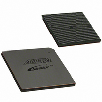
EP1S40F1508C5N Altera, EP1S40F1508C5N Datasheet - Page 231

EP1S40F1508C5N
Manufacturer Part Number
EP1S40F1508C5N
Description
IC STRATIX FPGA 40K LE 1508-FBGA
Manufacturer
Altera
Series
Stratix®r
Datasheet
1.EP1S10F780C7.pdf
(276 pages)
Specifications of EP1S40F1508C5N
Number Of Logic Elements/cells
41250
Number Of Labs/clbs
4125
Total Ram Bits
3423744
Number Of I /o
822
Voltage - Supply
1.425 V ~ 1.575 V
Mounting Type
Surface Mount
Operating Temperature
0°C ~ 85°C
Package / Case
1508-FBGA
Lead Free Status / RoHS Status
Lead free / RoHS Compliant
Number Of Gates
-
Available stocks
Company
Part Number
Manufacturer
Quantity
Price
Company:
Part Number:
EP1S40F1508C5N
Manufacturer:
ALTERA
Quantity:
300
- Current page: 231 of 276
- Download datasheet (4Mb)
Altera Corporation
January 2006
the FPGA device. The Quartus II software calculates the I/O timing for
each I/O standard with a default baseline loading as specified by the I/O
standard.
Altera measures clock-to-output delays (t
minimum voltage, and maximum temperature (PVT) for the 3.3-V LVTTL
I/O standard with 24 mA (default case) current drive strength setting and
fast slew rate setting. I/O adder delays are measured to calculate the t
change at worst-case PVT across all I/O standards and current drive
strength settings with the default loading shown in
page
across worst-case PVT for all I/O standards and drive strength settings.
These three pieces of data are used to predict the timing at the output pin.
Simulation using IBIS models is required to determine the delays on the
PCB traces in addition to the output pin delay timing reported by the
Quartus II software and the timing model in the device handbook.
1.
2.
3.
4.
5.
The Quartus II software reports maximum timing with the conditions
shown in
Figure 4–7 on page 4–62
by the Quartus II output timing.
t
Output Delay Adder for Loading
Simulate the output driver of choice into the generalized test setup
using values from
Record the time to VMEAS.
Simulate the output driver of choice into the actual PCB trace and
load, using the appropriate IBIS input buffer model or an equivalent
capacitance value to represent the load.
Record the time to VMEAS.
Compare the results of steps 2 and 4. The increase or decrease in
delay should be added to or subtracted from the I/O Standard
Output Adder delays to yield the actual worst-case propagation
delay (clock-to-input) of the PCB trace.
CO
4–62. Timing derating data for additional loading is taken for t
at pin = t
Table 4–101 on page 4–62
OUTCO
Table 4–101 on page
max for 3.3-V 24 mA LVTTL + I/O Adder +
shows the model of the circuit that is represented
using the proceeding equation.
Stratix Device Handbook, Volume 1
CO
DC & Switching Characteristics
) at worst-case process,
4–62.
Table 4–101 on
CO
4–61
CO
Related parts for EP1S40F1508C5N
Image
Part Number
Description
Manufacturer
Datasheet
Request
R

Part Number:
Description:
CYCLONE II STARTER KIT EP2C20N
Manufacturer:
Altera
Datasheet:

Part Number:
Description:
CPLD, EP610 Family, ECMOS Process, 300 Gates, 16 Macro Cells, 16 Reg., 16 User I/Os, 5V Supply, 35 Speed Grade, 24DIP
Manufacturer:
Altera Corporation
Datasheet:

Part Number:
Description:
CPLD, EP610 Family, ECMOS Process, 300 Gates, 16 Macro Cells, 16 Reg., 16 User I/Os, 5V Supply, 15 Speed Grade, 24DIP
Manufacturer:
Altera Corporation
Datasheet:

Part Number:
Description:
Manufacturer:
Altera Corporation
Datasheet:

Part Number:
Description:
CPLD, EP610 Family, ECMOS Process, 300 Gates, 16 Macro Cells, 16 Reg., 16 User I/Os, 5V Supply, 30 Speed Grade, 24DIP
Manufacturer:
Altera Corporation
Datasheet:

Part Number:
Description:
High-performance, low-power erasable programmable logic devices with 8 macrocells, 10ns
Manufacturer:
Altera Corporation
Datasheet:

Part Number:
Description:
High-performance, low-power erasable programmable logic devices with 8 macrocells, 7ns
Manufacturer:
Altera Corporation
Datasheet:

Part Number:
Description:
Classic EPLD
Manufacturer:
Altera Corporation
Datasheet:

Part Number:
Description:
High-performance, low-power erasable programmable logic devices with 8 macrocells, 10ns
Manufacturer:
Altera Corporation
Datasheet:

Part Number:
Description:
Manufacturer:
Altera Corporation
Datasheet:

Part Number:
Description:
Manufacturer:
Altera Corporation
Datasheet:

Part Number:
Description:
Manufacturer:
Altera Corporation
Datasheet:

Part Number:
Description:
CPLD, EP610 Family, ECMOS Process, 300 Gates, 16 Macro Cells, 16 Reg., 16 User I/Os, 5V Supply, 25 Speed Grade, 24DIP
Manufacturer:
Altera Corporation
Datasheet:


