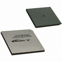
EP2S130F1508C3 Altera, EP2S130F1508C3 Datasheet - Page 121

EP2S130F1508C3
Manufacturer Part Number
EP2S130F1508C3
Description
IC STRATIX II FPGA 130K 1508FBGA
Manufacturer
Altera
Series
Stratix® IIr
Datasheet
1.EP2S15F484I4N.pdf
(238 pages)
Specifications of EP2S130F1508C3
Number Of Logic Elements/cells
132540
Number Of Labs/clbs
6627
Total Ram Bits
6747840
Number Of I /o
1126
Voltage - Supply
1.15 V ~ 1.25 V
Mounting Type
Surface Mount
Operating Temperature
0°C ~ 85°C
Package / Case
1508-FBGA
Family Name
Stratix II
Number Of Logic Blocks/elements
132540
# I/os (max)
1126
Frequency (max)
778.82MHz
Process Technology
90nm (CMOS)
Operating Supply Voltage (typ)
1.2V
Logic Cells
132540
Ram Bits
6747840
Operating Supply Voltage (min)
1.15V
Operating Supply Voltage (max)
1.25V
Operating Temp Range
0C to 85C
Operating Temperature Classification
Commercial
Mounting
Surface Mount
Pin Count
1508
Package Type
FC-FBGA
Lead Free Status / RoHS Status
Contains lead / RoHS non-compliant
Number Of Gates
-
Lead Free Status / Rohs Status
Not Compliant
Other names
544-2160
Available stocks
Company
Part Number
Manufacturer
Quantity
Price
Company:
Part Number:
EP2S130F1508C3
Manufacturer:
ALTERA
Quantity:
3 000
Part Number:
EP2S130F1508C3
Manufacturer:
ALTERA/阿尔特拉
Quantity:
20 000
Company:
Part Number:
EP2S130F1508C3N
Manufacturer:
ALTERA
Quantity:
216
Part Number:
EP2S130F1508C3N
Manufacturer:
ALTERA/阿尔特拉
Quantity:
20 000
Altera Corporation
May 2007
FPP
AS
PS
Configuration
Table 3–5. Stratix II Configuration Features (Part 1 of 2)
Scheme
MAX II device or microprocessor and
flash device
Enhanced configuration device
Serial configuration device
MAX II device or microprocessor and
flash device
Enhanced configuration device
Download cable
f
Configuration Method
you need to support configuration input voltages of 1.8 V/1.5 V, you
should set the VCCSEL to a logic high and the V
contains the configuration inputs to 1.8 V/1.5 V.
For more information on multi-volt support, including information on
using TDO and nCEO in multi-volt systems, refer to the Stratix II
Architecture chapter in volume 1 of the Stratix II Device Handbook.
Configuration Schemes
You can load the configuration data for a Stratix II device with one of five
configuration schemes (see
application. You can use a configuration device, intelligent controller, or
the JTAG port to configure a Stratix II device. A configuration device can
automatically configure a Stratix II device at system power-up.
You can configure multiple Stratix II devices in any of the five
configuration schemes by connecting the configuration enable (nCE) and
configuration enable output (nCEO) pins on each device.
Stratix II FPGAs offer the following:
■
■
■
Table 3–5
configuration scheme.
(4)
Configuration data decompression to reduce configuration file
storage
Design security using configuration data encryption to protect your
designs
Remote system upgrades for remotely updating your Stratix II
designs
summarizes which configuration features can be used in each
Design Security Decompression
Table
v
v
v
v
v
(1)
3–5), chosen on the basis of the target
Stratix II Device Handbook, Volume 1
v
v
v
v
v
v
CCIO
(1)
(2)
Configuration & Testing
of the bank that
Remote System
Upgrade
v
v
v
v
v
(3)
3–7


