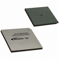
EP2S130F1508I4 Altera, EP2S130F1508I4 Datasheet - Page 233

EP2S130F1508I4
Manufacturer Part Number
EP2S130F1508I4
Description
IC STRATIX II FPGA 130K 1508FBGA
Manufacturer
Altera
Series
Stratix® IIr
Datasheet
1.EP2S15F484I4N.pdf
(238 pages)
Specifications of EP2S130F1508I4
Number Of Logic Elements/cells
132540
Number Of Labs/clbs
6627
Total Ram Bits
6747840
Number Of I /o
1126
Voltage - Supply
1.15 V ~ 1.25 V
Mounting Type
Surface Mount
Operating Temperature
-40°C ~ 100°C
Package / Case
1508-FBGA
Lead Free Status / RoHS Status
Contains lead / RoHS non-compliant
Number Of Gates
-
Other names
544-2161
Available stocks
Company
Part Number
Manufacturer
Quantity
Price
Company:
Part Number:
EP2S130F1508I4
Manufacturer:
ALTERA
Quantity:
3 000
Part Number:
EP2S130F1508I4
Manufacturer:
ALTERA/阿尔特拉
Quantity:
20 000
Company:
Part Number:
EP2S130F1508I4N
Manufacturer:
ALTERA
Quantity:
650
Part Number:
EP2S130F1508I4N
Manufacturer:
ALTERA/阿尔特拉
Quantity:
20 000
Document
Revision History
Altera Corporation
April 2011
April 2011, v4.5
July 2009, v4.4
May 2007, v4.3
Table 5–103. Document Revision History (Part 1 of 3)
Document
Date and
Version
Updated
Updated
●
●
●
Moved the Document Revision History section to the
end of the chapter.
Updated R
Updated f
Updated f
Table
Table
Table 5–102
devices.
Table 5–103
Note to
(1)
t
t
t
t
t
t
t
t
Symbol
JCP
JCH
JCL
JPSU
JPH
JPCO
JPZX
JPXZ
Table 5–102. Stratix II JTAG Timing Parameters & Values
IN
IN
CONF
5–3.
5–92.
(min) in Table 5–92.
and f
A 1 ns adder is required for each V
example,
1.8 V.
in Table 5–4.
Changes Made
Table
INPFD
TCK
TCK
TCK
JTAG port setup time
JTAG port hold time
JTAG port clock to output
JTAG port high impedance to valid output
JTAG port valid output to high impedance
shows the JTAG timing parameters and values for Stratix II
shows the revision history for this chapter.
t
5–102:
in Table 5–93.
JPCO
clock period
clock high time
clock low time
= 12 ns if V
Parameter
C C I O
of the TDO I/O bank = 2.5 V, or 13 ns if it equals
C C I O
Stratix II Device Handbook, Volume 1
voltage step down from 3.3 V. For
Added operating junction temperature
for military use.
Updated the spread spectrum
modulation frequency (f
(100 kHz–500 kHz) to
(30 kHz–150 kHz).
DC & Switching Characteristics
Summary of Changes
Min
13
13
30
3
5
—
—
11
14
14
Max
(1)
(1)
(1)
S S
) from
Unit
ns
ns
ns
ns
ns
ns
ns
ns
5–97


