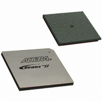
EP2SGX130GF1508I4 Altera, EP2SGX130GF1508I4 Datasheet - Page 235

EP2SGX130GF1508I4
Manufacturer Part Number
EP2SGX130GF1508I4
Description
IC STRATIX II GX 130K 1508-FBGA
Manufacturer
Altera
Series
Stratix® II GXr
Datasheet
1.EP2SGX30DF780C5.pdf
(316 pages)
Specifications of EP2SGX130GF1508I4
Number Of Logic Elements/cells
132540
Number Of Labs/clbs
6627
Total Ram Bits
6747840
Number Of I /o
734
Voltage - Supply
1.15 V ~ 1.25 V
Mounting Type
Surface Mount
Operating Temperature
-40°C ~ 100°C
Package / Case
1508-FBGA
Family Name
Stratix II GX
Number Of Logic Blocks/elements
132540
# I/os (max)
734
Frequency (max)
732.1MHz
Process Technology
SRAM
Operating Supply Voltage (typ)
1.2V
Logic Cells
132540
Ram Bits
6747840
Operating Supply Voltage (min)
1.15V
Operating Supply Voltage (max)
1.25V
Operating Temp Range
-40C to 100C
Operating Temperature Classification
Industrial
Mounting
Surface Mount
Pin Count
1508
Package Type
FC-FBGA
Lead Free Status / RoHS Status
Contains lead / RoHS non-compliant
Number Of Gates
-
Lead Free Status / Rohs Status
Not Compliant
Other names
544-2174
Available stocks
Company
Part Number
Manufacturer
Quantity
Price
Company:
Part Number:
EP2SGX130GF1508I4N
Manufacturer:
Sunon
Quantity:
1 000
Part Number:
EP2SGX130GF1508I4N
Manufacturer:
ALTERA/阿尔特拉
Quantity:
20 000
- Current page: 235 of 316
- Download datasheet (2Mb)
Altera Corporation
June 2009
Notes to
(1)
(2)
(3)
(4)
(5)
(6)
1.8-V HSTL Class II
1.5-V HSTL Class I
1.5-V HSTL Class II
1.2-V HSTL with OCT
Differential SSTL-2 Class I
Differential SSTL-2 Class II
Differential SSTL-18 Class I
Differential SSTL-18 Class II
1.5-V differential HSTL Class I
1.5-V differential HSTL Class II
1.8-V differential HSTL Class I
1.8-V differential HSTL Class II
LVDS
LVPECL
Table 4–54. Timing Measurement Methodology for Input Pins (Part 2 of 2)
Input buffer sees no load at buffer input.
Input measuring point at buffer input is 0.5 V
Output measuring point is 0.5 V
Input edge rate is 1 V/ns.
Less than 50-mV ripple on V
V
CCPD
Table
= 2.97 V, less than 50-mV ripple on V
I/O Standard
4–54:
CCIO
CC
and V
at internal node.
CCPD
V
CCIO
, V
CCIO
1.660
1.375
1.375
1.140
2.325
2.325
1.660
1.660
1.375
1.375
1.660
1.660
2.325
3.135
CCIO
CCINT
and V
(V)
.
Measurement Conditions
= 1.15 V with less than 30-mV ripple.
CCPD
, V
V
0.830
0.688
0.688
0.570
1.163
1.163
0.830
0.830
0.688
0.688
0.830
0.830
REF
CCINT
(V)
= 1.15 V.
Stratix II GX Device Handbook, Volume 1
Edge Rate (ns)
DC and Switching Characteristics
1.660
1.375
1.375
1.140
2.325
2.325
1.660
1.660
1.375
1.375
1.660
1.660
0.100
0.100
Notes
(1), (2), (3),
Measurement Point
VMEAS (V)
0.6875
0.6875
1.1625
1.1625
0.6875
0.6875
1.1625
1.5675
0.570
0.83
0.83
0.83
0.83
0.83
(4)
4–65
Related parts for EP2SGX130GF1508I4
Image
Part Number
Description
Manufacturer
Datasheet
Request
R

Part Number:
Description:
CYCLONE II STARTER KIT EP2C20N
Manufacturer:
Altera
Datasheet:

Part Number:
Description:
CPLD, EP610 Family, ECMOS Process, 300 Gates, 16 Macro Cells, 16 Reg., 16 User I/Os, 5V Supply, 35 Speed Grade, 24DIP
Manufacturer:
Altera Corporation
Datasheet:

Part Number:
Description:
CPLD, EP610 Family, ECMOS Process, 300 Gates, 16 Macro Cells, 16 Reg., 16 User I/Os, 5V Supply, 15 Speed Grade, 24DIP
Manufacturer:
Altera Corporation
Datasheet:

Part Number:
Description:
Manufacturer:
Altera Corporation
Datasheet:

Part Number:
Description:
CPLD, EP610 Family, ECMOS Process, 300 Gates, 16 Macro Cells, 16 Reg., 16 User I/Os, 5V Supply, 30 Speed Grade, 24DIP
Manufacturer:
Altera Corporation
Datasheet:

Part Number:
Description:
High-performance, low-power erasable programmable logic devices with 8 macrocells, 10ns
Manufacturer:
Altera Corporation
Datasheet:

Part Number:
Description:
High-performance, low-power erasable programmable logic devices with 8 macrocells, 7ns
Manufacturer:
Altera Corporation
Datasheet:

Part Number:
Description:
Classic EPLD
Manufacturer:
Altera Corporation
Datasheet:

Part Number:
Description:
High-performance, low-power erasable programmable logic devices with 8 macrocells, 10ns
Manufacturer:
Altera Corporation
Datasheet:

Part Number:
Description:
Manufacturer:
Altera Corporation
Datasheet:

Part Number:
Description:
Manufacturer:
Altera Corporation
Datasheet:

Part Number:
Description:
Manufacturer:
Altera Corporation
Datasheet:

Part Number:
Description:
CPLD, EP610 Family, ECMOS Process, 300 Gates, 16 Macro Cells, 16 Reg., 16 User I/Os, 5V Supply, 25 Speed Grade, 24DIP
Manufacturer:
Altera Corporation
Datasheet:


