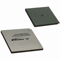
EP2S180F1508I4 Altera, EP2S180F1508I4 Datasheet - Page 219

EP2S180F1508I4
Manufacturer Part Number
EP2S180F1508I4
Description
IC STRATIX II FPGA 180K 1508FBGA
Manufacturer
Altera
Series
Stratix® IIr
Datasheet
1.EP2S15F484I4N.pdf
(238 pages)
Specifications of EP2S180F1508I4
Number Of Logic Elements/cells
179400
Number Of Labs/clbs
8970
Total Ram Bits
9383040
Number Of I /o
1170
Voltage - Supply
1.15 V ~ 1.25 V
Mounting Type
Surface Mount
Operating Temperature
-40°C ~ 100°C
Package / Case
1508-FBGA
Family Name
Stratix II
Number Of Logic Blocks/elements
179400
# I/os (max)
1170
Frequency (max)
711.24MHz
Process Technology
90nm (CMOS)
Operating Supply Voltage (typ)
1.2V
Logic Cells
179400
Ram Bits
9383040
Operating Supply Voltage (min)
1.15V
Operating Supply Voltage (max)
1.25V
Operating Temp Range
-40C to 100C
Operating Temperature Classification
Industrial
Mounting
Surface Mount
Pin Count
1508
Package Type
FC-FBGA
For Use With
544-1701 - DSP PRO KIT W/SII EP2S180N
Lead Free Status / RoHS Status
Contains lead / RoHS non-compliant
Number Of Gates
-
Lead Free Status / Rohs Status
Not Compliant
Other names
544-2165
Available stocks
Company
Part Number
Manufacturer
Quantity
Price
Company:
Part Number:
EP2S180F1508I4
Manufacturer:
ALTERA
Quantity:
3 000
Part Number:
EP2S180F1508I4
Manufacturer:
ALTERA/阿尔特拉
Quantity:
20 000
Company:
Part Number:
EP2S180F1508I4N
Manufacturer:
ALTERA
Quantity:
238
Part Number:
EP2S180F1508I4N
Manufacturer:
ALTERA/阿尔特拉
Quantity:
20 000
Altera Corporation
April 2011
Notes to
(1)
(2)
3.3-V LVTTL
3.3-V LVCMOS
2.5 V
1.8 V
1.5-V LVCMOS
SSTL-2 Class I
SSTL-2 Class II
SSTL-18 Class I
1.8-V HSTL Class I
1.5-V HSTL Class I
LVDS/ HyperTransport
technology
3.3-V LVTTL
3.3-V LVCMOS
2.5 V
DDIO Column Output I/O
Table 5–83. Maximum DCD for DDIO Output on Row I/O Pins Without PLL in the Clock Path for -4 & -5
Devices
Table 5–84. Maximum DCD for DDIO Output on Column I/O Pins Without PLL in the Clock Path for -3
Devices (Part 1 of 2)
Row DDIO Output I/O
Table 5–83
The DCD specification is based on a no logic array noise condition.
Standard
Standard
Table
Notes
5–83:
assumes the input clock has zero DCD.
(1),
(2)
Maximum DCD Based on I/O Standard of Input Feeding the DDIO Clock
3.3/2.5 V
Notes
Maximum DCD Based on I/O Standard of Input Feeding the DDIO
3.3/2.5 V
Therefore, the DCD percentage for the 267 MHz SSTL-2 Class II DDIO
row output clock on a –3 device ranges from 48.4% to 51.6%.
440
390
375
325
430
355
350
335
330
330
180
260
210
195
TTL/CMOS
(1),
TTL/CMOS
(2)
1.8/1.5 V
Clock Port (No PLL in the Clock Path)
1.8/1.5 V
495
450
430
385
490
410
405
390
385
390
180
Port (No PLL in the Clock Path)
380
330
315
SSTL-2
2.5 V
170
120
105
160
180
90
85
80
65
60
60
SSTL-2
2.5 V
145
100
85
SSTL/HSTL
1.8/1.5 V
160
110
100
155
180
SSTL/HSTL
95
75
70
65
70
70
Stratix II Device Handbook, Volume 1
1.8/1.5 V
145
100
85
DC & Switching Characteristics
HyperTransport
Technology
LVDS/
3.3 V
105
135
100
105
110
105
180
75
90
85
90
1.2-V
HSTL
1.2 V
145
100
85
Unit
ps
ps
ps
Unit
ps
ps
ps
ps
ps
ps
ps
ps
ps
ps
ps
5–83


