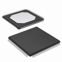
XC3S50-5TQG144C Xilinx Inc, XC3S50-5TQG144C Datasheet - Page 52

XC3S50-5TQG144C
Manufacturer Part Number
XC3S50-5TQG144C
Description
SPARTAN-3A FPGA 50K 144-TQFP
Manufacturer
Xilinx Inc
Series
Spartan™-3r
Datasheet
1.XC3S50-4VQG100C.pdf
(217 pages)
Specifications of XC3S50-5TQG144C
Total Ram Bits
73728
Number Of Logic Elements/cells
1728
Number Of Labs/clbs
192
Number Of I /o
97
Number Of Gates
50000
Voltage - Supply
1.14 V ~ 1.26 V
Mounting Type
Surface Mount
Operating Temperature
0°C ~ 85°C
Package / Case
144-LQFP
No. Of Logic Blocks
1728
No. Of Gates
50000
No. Of Macrocells
1728
No. Of Speed Grades
5
No. Of I/o's
97
Clock Management
DLL
Lead Free Status / RoHS Status
Lead free / RoHS Compliant
Available stocks
Company
Part Number
Manufacturer
Quantity
Price
- Current page: 52 of 217
- Download datasheet (6Mb)
S p ar t an -3 FP G A Fam ily : Fu n c t io n al D es c r ip t i o n
Configuration is automatically initiated after power-on
unless it is delayed by the user. INIT_B is an open-drain line
that the FPGA holds Low during the clearing of the configu-
ration memory. Extending the time that the pin is Low
causes the configuration sequencer to wait. Thus, configu-
ration is delayed by preventing entry into the phase where
data is loaded.
The configuration process can also be initiated by asserting
the PROG_B pin. The end of the memory-clearing phase is
signaled by the INIT_B pin going High. At this point, the con-
figuration data is written to the FPGA. The FPGA pulses the
Global Set/Reset (GSR) signal at the end of configuration,
resetting all flip-flops. The completion of the entire process
is signaled by the DONE pin going High.
The default start-up sequence, shown in
as a transition to the User mode. The default start-up
sequence is that one CCLK cycle after DONE goes High,
the Global Three-State signal (GTS) is released. This per-
mits device outputs to which signals have been assigned to
52
54
Start-Up Clock
Start-Up Clock
Notes:
1.
Figure 29: Default Start-Up Sequence
The BitGen option StartupClk in the Xilinx
development software selects the CCLK input,
TCK input, or a user-designated clock input (via the
STARTUP_SPARTAN3 primitive) for receiving the
clock signal that synchronizes Start-Up.
DONE
DONE
Phase
Phase
GWE
GWE
GTS
GTS
DONE High
0
0
1
1
Default Cycles
Sync-to-DONE
2
2
3
3
4
4
5
5
Figure
DS099_028_060905
6 7
6 7
29, serves
www.xilinx.com
become active. One CCLK cycle later, the Global Write
Enable (GWE) signal is released. This permits the internal
storage elements to begin changing state in response to the
design logic and the user clock.
The relative timing of configuration events can be changed
via the BitGen options in the Xilinx development software. In
addition, the GTS and GWE events can be made depen-
dent on the DONE pins of multiple devices all going High,
forcing the devices to start synchronously. The sequence
can also be paused at any stage, until lock has been
achieved on any DCM.
Readback
Using Slave Parallel mode, configuration data from the
FPGA can be read back. Readback is supported only in the
Slave Parallel and Boundary-Scan modes.
Along with the configuration data, it is possible to read back
the contents of all registers, distributed RAM, and block
RAM resources. This capability is used for real-time debug-
ging.
Additional Configuration Details
Additional details about the Spartan-3 FPGA configuration
architecture and command set are available in the “Spar-
tan-3 Generation Configuration User Guide” (
the "Spartan-3 Advanced Configuration Architecture" appli-
cation note (
Powering Spartan-3 FPGAs
Voltage Regulators
Various power supply manufacturers offer complete power
solutions for Xilinx FPGAs, including some with integrated
multi-rail regulators specifically designed for Spartan-3
FPGAs. The
vendor solution guides as well as Xilinx power estimation
and analysis tools.
Power Distribution System (PDS) Design and
Bypass/Decoupling Capacitors
Good power distribution system (PDS) design is important
for all FPGA designs, especially for high-performance appli-
cations. Proper design results in better overall performance,
lower clock and DCM jitter, and a generally more robust sys-
tem. Before designing the printed circuit board (PCB) for the
FPGA design, review "Power Distribution System (PDS)
Design: Using Bypass/Decoupling Capacitors" (
Power-On Behavior
Spartan-3 FPGAs have a built-in Power-On Reset (POR)
circuit that monitors the three power rails required to suc-
cessfully configure the FPGA. At power-up, the POR circuit
holds the FPGA in a reset state until the V
and V
CCO
Bank 4 supplies reach their respective input
XAPP452
Xilinx Power Corner
).
DS099-2 (v2.5) December 4, 2009
website provides links to
Product Specification
CCINT
UG332
XAPP623
, V
CCAUX
) and
).
R
,
Related parts for XC3S50-5TQG144C
Image
Part Number
Description
Manufacturer
Datasheet
Request
R

Part Number:
Description:
FPGA Spartan®-3 Family 50K Gates 1728 Cells 630MHz 90nm Technology 1.2V 144-Pin TQFP
Manufacturer:
Xilinx Inc
Datasheet:

Part Number:
Description:
FPGA Spartan®-3 Family 50K Gates 1728 Cells 630MHz 90nm Technology 1.2V 144-Pin TQFP
Manufacturer:
Xilinx Inc
Datasheet:

Part Number:
Description:
FPGA Spartan®-3 Family 50K Gates 1728 Cells 630MHz 90nm Technology 1.2V 100-Pin VTQFP
Manufacturer:
Xilinx Inc
Datasheet:

Part Number:
Description:
FPGA Spartan®-3 Family 50K Gates 1728 Cells 630MHz 90nm Technology 1.2V 144-Pin TQFP
Manufacturer:
Xilinx Inc
Datasheet:

Part Number:
Description:
SPARTAN-3A FPGA 50K 100-VQFP
Manufacturer:
Xilinx Inc
Datasheet:

Part Number:
Description:
SPARTAN-3A FPGA 50K STD 100-VQFP
Manufacturer:
Xilinx Inc
Datasheet:

Part Number:
Description:
SPARTAN-3A FPGA 50K STD 208-PQFP
Manufacturer:
Xilinx Inc
Datasheet:

Part Number:
Description:
SPARTAN-3A FPGA 50K 208-PQFP
Manufacturer:
Xilinx Inc
Datasheet:

Part Number:
Description:
SPARTAN-3A FPGA 50K STD 208-PQFP
Manufacturer:
Xilinx Inc
Datasheet:

Part Number:
Description:
SPARTAN-3A FPGA 50K 132-CSBGA
Manufacturer:
Xilinx Inc
Datasheet:

Part Number:
Description:
SPARTAN-3A FPGA 50K STD 132CSBGA
Manufacturer:
Xilinx Inc
Datasheet:

Part Number:
Description:
SPARTAN-3A FPGA 50K STD 132CSBGA
Manufacturer:
Xilinx Inc
Datasheet:

Part Number:
Description:
FPGA Spartan®-3 Family 50K Gates 1728 Cells 630MHz 90nm Technology 1.2V 100-Pin VTQFP
Manufacturer:
Xilinx Inc
Datasheet:

Part Number:
Description:
IC CPLD .8K 36MCELL 44-VQFP
Manufacturer:
Xilinx Inc
Datasheet:


