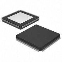
XC3S50-5PQG208C Xilinx Inc, XC3S50-5PQG208C Datasheet - Page 100

XC3S50-5PQG208C
Manufacturer Part Number
XC3S50-5PQG208C
Description
SPARTAN-3A FPGA 50K 208-PQFP
Manufacturer
Xilinx Inc
Series
Spartan™-3r
Datasheet
1.XC3S50-4VQG100C.pdf
(217 pages)
Specifications of XC3S50-5PQG208C
Number Of Logic Elements/cells
1728
Number Of Labs/clbs
192
Total Ram Bits
73728
Number Of I /o
124
Number Of Gates
50000
Voltage - Supply
1.14 V ~ 1.26 V
Mounting Type
Surface Mount
Operating Temperature
0°C ~ 85°C
Package / Case
208-BFQFP
Lead Free Status / RoHS Status
Lead free / RoHS Compliant
Available stocks
Company
Part Number
Manufacturer
Quantity
Price
Part Number:
XC3S50-5PQG208C
Manufacturer:
XILINX/赛灵思
Quantity:
20 000
- Current page: 100 of 217
- Download datasheet (6Mb)
Spartan-3 FPGA Family: Pinout Descriptions
Table 68: Types of Pins on Spartan-3 FPGAs (Continued)
I/Os with Lxxy_# are part of a differential output pair. ‘L’ indi-
cates differential output capability. The “xx” field is a
two-digit integer, unique to each bank that identifies a differ-
ential pin-pair. The ‘y’ field is either ‘P’ for the true signal or
‘N’ for the inverted signal in the differential pair. The ‘#’ field
is the I/O bank number.
100
Notes:
1.
VCCAUX
VCCINT
VCCO
VREF
GCLK
Type/
Color
Code
GND
N.C.
# = I/O bank number, an integer between 0 and 7.
Dual-purpose pin that is either a user-I/O pin or, along with all other VREF
pins in the same bank, provides a reference voltage input for certain I/O
standards. If used for a reference voltage within a bank, all VREF pins
within the bank must be connected.
Dedicated ground pin. The number of GND pins depends on the package
used. All must be connected.
Dedicated auxiliary power supply pin. The number of VCCAUX pins
depends on the package used. All must be connected to +2.5V.
Dedicated internal core logic power supply pin. The number of VCCINT
pins depends on the package used. All must be connected to +1.2V.
Dedicated I/O bank, output buffer power supply pin. Along with other
VCCO pins in the same bank, this pin supplies power to the output buffers
within the I/O bank and sets the input threshold voltage for some I/O
standards.
Dual-purpose pin that is either a user-I/O pin or an input to a specific global
buffer input. Every package has eight dedicated GCLK pins.
This package pin is not connected in this specific device/package
combination but may be connected in larger devices in the same package.
Description
www.xilinx.com
Pin Definitions
Table 69
Spartan-3 FPGA pinout tables and package footprint dia-
grams. Pins are categorized by their pin type, as listed in
Table
more information.
68. See
provides a brief description of each pin listed in the
Detailed, Functional Pin Descriptions
IO/VREF_#
IO_Lxxy_#/VREF_#
GND
VCCAUX
VCCINT
VCCO_#
CP132 and TQ144 Packages
Only:
VCCO_LEFT, VCCO_TOP,
VCCO_RIGHT,
VCCO_BOTTOM
IO_Lxxy_#/GCLK0,
IO_Lxxy_#/GCLK1,
IO_Lxxy_#/GCLK2,
IO_Lxxy_#/GCLK3,
IO_Lxxy_#/GCLK4,
IO_Lxxy_#/GCLK5,
IO_Lxxy_#/GCLK6,
IO_Lxxy_#/GCLK7
N.C.
DS099-4 (v2.5) December 4, 2009
Pin Name(s) in Type
Product Specification
for
R
Related parts for XC3S50-5PQG208C
Image
Part Number
Description
Manufacturer
Datasheet
Request
R

Part Number:
Description:
FPGA Spartan®-3 Family 50K Gates 1728 Cells 630MHz 90nm Technology 1.2V 144-Pin TQFP
Manufacturer:
Xilinx Inc
Datasheet:

Part Number:
Description:
SPARTAN-3A FPGA 50K 144-TQFP
Manufacturer:
Xilinx Inc
Datasheet:

Part Number:
Description:
FPGA Spartan®-3 Family 50K Gates 1728 Cells 630MHz 90nm Technology 1.2V 144-Pin TQFP
Manufacturer:
Xilinx Inc
Datasheet:

Part Number:
Description:
FPGA Spartan®-3 Family 50K Gates 1728 Cells 630MHz 90nm Technology 1.2V 100-Pin VTQFP
Manufacturer:
Xilinx Inc
Datasheet:

Part Number:
Description:
FPGA Spartan®-3 Family 50K Gates 1728 Cells 630MHz 90nm Technology 1.2V 144-Pin TQFP
Manufacturer:
Xilinx Inc
Datasheet:

Part Number:
Description:
SPARTAN-3A FPGA 50K 100-VQFP
Manufacturer:
Xilinx Inc
Datasheet:

Part Number:
Description:
SPARTAN-3A FPGA 50K STD 100-VQFP
Manufacturer:
Xilinx Inc
Datasheet:

Part Number:
Description:
SPARTAN-3A FPGA 50K STD 208-PQFP
Manufacturer:
Xilinx Inc
Datasheet:

Part Number:
Description:
SPARTAN-3A FPGA 50K STD 208-PQFP
Manufacturer:
Xilinx Inc
Datasheet:

Part Number:
Description:
SPARTAN-3A FPGA 50K 132-CSBGA
Manufacturer:
Xilinx Inc
Datasheet:

Part Number:
Description:
SPARTAN-3A FPGA 50K STD 132CSBGA
Manufacturer:
Xilinx Inc
Datasheet:

Part Number:
Description:
SPARTAN-3A FPGA 50K STD 132CSBGA
Manufacturer:
Xilinx Inc
Datasheet:

Part Number:
Description:
FPGA Spartan®-3 Family 50K Gates 1728 Cells 630MHz 90nm Technology 1.2V 100-Pin VTQFP
Manufacturer:
Xilinx Inc
Datasheet:

Part Number:
Description:
IC CPLD .8K 36MCELL 44-VQFP
Manufacturer:
Xilinx Inc
Datasheet:


