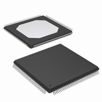
XCS20XL-4TQ144I Xilinx Inc, XCS20XL-4TQ144I Datasheet - Page 15

XCS20XL-4TQ144I
Manufacturer Part Number
XCS20XL-4TQ144I
Description
IC FPGA 3.3V I-TEMP HP 144TQFP
Manufacturer
Xilinx Inc
Series
Spartan™-XLr
Datasheet
1.XCS05XL-4VQG100C.pdf
(83 pages)
Specifications of XCS20XL-4TQ144I
Number Of Logic Elements/cells
950
Number Of Labs/clbs
400
Total Ram Bits
12800
Number Of I /o
113
Number Of Gates
20000
Voltage - Supply
3 V ~ 3.6 V
Mounting Type
Surface Mount
Operating Temperature
-40°C ~ 100°C
Package / Case
144-LQFP
Lead Free Status / RoHS Status
Contains lead / RoHS non-compliant
Available stocks
Company
Part Number
Manufacturer
Quantity
Price
Company:
Part Number:
XCS20XL-4TQ144I
Manufacturer:
XILINX
Quantity:
252
Part Number:
XCS20XL-4TQ144I
Manufacturer:
XILINX/赛灵思
Quantity:
20 000
WCLK can be configured as active on either the rising edge
(default) or the falling edge. While the WCLK input to the
RAM accepts the same signal as the clock input to the asso-
ciated CLB’s flip-flops, the sense of this WCLK input can be
DS060 (v1.8) June 26, 2008
Product Specification
DATA OUT
ADDRESS
WCLK (K)
DATA IN
Figure 13: Data Write and Access Timing for RAM
WE
R
WCLK
A[3:0]
T
WE
ILO
D
T
T
T
WSS
DSS
ASS
4
Figure 14: Logic Diagram for the Dual-Port RAM
OLD
T
T
WOS
T
T
DHS
WHS
AHS
T
WPS
NEW
4
T
DS060_13_080400
ILO
www.xilinx.com
4
inverted with respect to the sense of the flip-flop clock
inputs. Consequently, within the same CLB, data at the
RAM SPO line can be stored in a flip-flop with either the
same or the inverse clock polarity used to write data to the
RAM.
The WE input is active High and cannot be inverted within
the CLB.
Allowing for settling time, the data on the SPO output
reflects the contents of the RAM location currently
addressed. When the address changes, following the asyn-
chronous delay T
location will appear on SPO. If the data at a particular RAM
address is overwritten, after the delay T
will appear on SPO.
Dual-Port Mode
In dual-port mode, the function generators (F-LUT and
G-LUT) are used to create a 16 x 1 dual-port memory. Of
the two data ports available, one permits read and write
operations at the address specified by A[3:0] while the sec-
ond provides only for read operations at the address speci-
fied independently by DPRA[3:0]. As a result, simultaneous
read/write operations at different addresses (or even at the
same address) are supported.
The functional organization of the 16 x 1 dual-port RAM is
shown in
CONTROL
CONTROL
WRITE
WRITE
Spartan and Spartan-XL FPGA Families Data Sheet
16 x 1
16 x 1
RAM
RAM
Figure
READ
READ
OUT
OUT
14. The dual-port RAM signals and the
ILO
, the data stored at the new address
4
DS060_14_043001
DPRA[3:0]
SPO
DPO
WOS
, the new data
15


